The 2025.6 Silicon Labs SSDK Z-Wave release changes the familiar DEBUGPRINT utility to ZPAL_LOG. A brief mention of the change is in the Important Changes for the Z-Wave 7.24.0 release however I’ll give a more detailed description of what has changed and how to use this new utility. If you’re trying to upgrade a project from an earlier SDK, this “breaking change” will make that effort more difficult as you have to switch any DPRINT statements to the new ZPAL_LOG format.
DEBUGPRINT
First a little history. The DEBUGPRINT utility came from the original early 2000s Zensys code running on the 8051 8-bit CPU. From the initial 100 series thru the 500 series, DEBUGPRINT was the ONLY debug utility we had! Even though this was the 2000s thru most of the 2010s, debugging using PRINTF was obsolete by the late 1980s – but not for Z-Wave. PRINTF would print out a short message and maybe a hex value or two and we would try to divine what was going on from these tiny details. There were no breakpoints, no ability to single step the CPU or watch RAM or registers change as the code was executing. Because sending characters out the UART would block the CPU until the UART was empty, you could only send a few characters and maybe a hex value. Sending more characters out the UART would alter the flow of the program and either mask the bug or break something else or often cause a watchdog reset! UGH. While primitive, it was all we had and we made do. DEBUGPRINT was easy to enable or disable – just #define DEBUGPRINT in the file you needed the print statements and recompile. Typically, only a few print statements were enabled at a time or the UART would spew out too much detail or messages would get mixed together making gibberish of the output.
Debugging Today
Debug is much easier with the modern ARM CM33 processor on todays Z-Wave chips. We have Single-Wire-Debug (SWD) and can set breakpoints, watchpoints, single step, view memory and peripherals. There’s even Trace where every instruction executed is logged enabling the precise flow of a program to be viewed after the trigger condition of a bug. We still have DEBUGPRINT which is handy for printing out high level messages like “eReset Reason=3′ each time the chip reboots. These messages are handy during debug and were easy to remove prior to building the final production code simply by commenting out the #define.
ZPAL_LOG
The Z-Wave Log component in a Simplicity Studio project .slcp file is installed by default in all the sample applications starting with the 7.24 release. This is good thing and a bad thing. It’s good since it’s already installed and printing messages before you’ve started modifying the code for your project. It’s bad because when you should remove this code for the final production build, we’ll get into that shortly.
General
When you Configure the Z-Wave Log component you get a lot of radio buttons to switch various features on or off. The first block “General” includes:
Size of the buffer (default is 96 bytes) – Leave this as-is
Display log level – prints 3 characters identifying Info, Debug, Warnings or Error messages
Display log source component – prints a number which identifes which module the print statement is from
Display log timestamp – prints a decimal number of ticks since reset
Enabling any of these messages slightly increases the total FLASH usage. The bigger problem is that it increases the number of characters sent out the UART potentially causing the CPU to block and thus changing the program flow. I recommend leaving these at their defaults.
The Display Log Source component would be useful IF SSv5 decoded the numeric value for you and displayed the name in the console window. Unfortunately it just prints a number which you then must manually decode by looking up the value in the enumerated type zpal_log_component in the zpal_log.h file. The trick would be to send just the numeric number out the UART (thus not taking up significant amounts of time or FLASH) and then SSv5 expanding it to the component name. I have suggested this to the SSv5 team in the past but hasn’t yet come to fruition. The source component is useful if there are several similar or even identical PRINT statements in different blocks of code to help identify where it is coming from. Also if you enable a lot of PRINT statements, it can help narrow down which block a specific message is coming from.
If you enable all 3 of these switches you get: “000000023 [I] (1) ApplicationInit eResetReason = 7”. Where the 00000023 is the timestamp; [i] is the Log Level (Info in this case) and (1) is the component which you have to then decode yourself as mentioned above (ZPAL_LOG_APP in this case) .
Output Channels
The next block is the Output Channels which can enable the four levels of messages: Debug, Info, Warning and Error messages. The default has just Info enabled with the word “vcom” entered into the Info box. I recommend enabling all four of these by entering “vcom” into all four of them. This will increase FLASH usage as the strings for all these messages are now stored on-chip.
Component Filtering
The final configuration block in the Z-Wave Log component is the Component Filtering section. This section has a bunch of radio buttons you can enable which will turn on various messages from the respective module. If you enable ALL of these, it’ll add about 10K bytes of FLASH so maybe only enable ones you think you need.
UART Blocking
The EUSART is only running at 115200 baud which makes each character take over 10 microseconds to send out the UART. This might seem fast, but when you’re transmitting long strings of characters this can seriously impact the program flow in real time. If the UART buffer fills, the code will stall and wait for more buffer space to fill (see the “while” loop in eusart_tx in sl_iostream_eusart.c). If you’re spitting out a lot of messages, the UART will fill causing the program flow to change potentially masking the bug or sending you down the wrong rathole. The baud rate is easily increased to 1mbps which will speed up the printing by 10X which helps, but you need to be aware of the amount of messages pouring out the limited speed of the UART.
Disabling ZPAL_LOG
Once debugging is complete, the next step is to compile all of these messages out of the production code. Fortunately this is easy – just remove “vcom” from all four of the Output Channels section of the Z-Wave Log component. While this removes most of the code for debug messages, the Command Line Interface (CLI) is still there and the EUSART is still used by the sample applications. When developing your own application you will typically want to remove ZPAL_LOG and the CLI as it’s not something your application needs – it is only for the Silicon Labs demos.
Conclusion
Why did silabs make this “breaking change”? I don’t have specific insights from Silicon Labs but the new format provides easily configured “levels” of logging. Is that worth a “breaking change”? I wish they’d spend more time testing the code to reduce the bugs than making a lot of file changes tweaking features that don’t really improve the developers experience. If you’re going to change an important feature, it’s also important to document it which is sorely lacking. But I hope this post helps you utilize this new feature and not be quite so frustrated when updating your project to the latest SDK.
The EFR32ZG23 Z-Wave 800 series MCU has limited FLASH and RAM available for the application. The 800 series actually has less FLASH than the 700 series which stored the bootloader in a dedicated 16K memory. Worse, the bootloader in the 800 series has grown from 16K to 24K! Features are always being added to the SDK making it ever larger leaving less for the application. Seems like Silicon Labs needs to spend some time squeezing the code instead of constantly adding features.
Here is the typical error message when FLASH overflows:
Description
FLASH memory overflowed !
make: *** [makefile:114: all] Error 2
make[1]: *** [makefile:123: SwOnOff_2024120_ZG23B_GeoLoc.axf] Error 1
region `FLASH' overflowed by 92 bytes
SwOnOff_2024120_ZG23B_GeoLoc.axf section `.nvm' will not fit in region `FLASH'
We can’t create more FLASH on the chip, it has what it has. But, there’s always software we can change! By default, the project has ZAF->Z-Wave Release installed which sets the C compiler optimization to -Os which optimizes for size which is probably what we want since we’re out of FLASH. However, deep in the configuration files there is the definition for SL_BOOTLOADER_STORAGE_SIZE which changes from 196K to 180Kbytes when NDEBUG is defined. NDEBUG is defined when the Z-Wave->ZAF->Z-Wave Debug component is installed. The question of why BOOTLOADER size is being reduced by only 16K when debug is enabled is unclear to me. However, in my testing, adding the DEBUG component still results in FLASH overflowing but now by 4344 bytes! Obviously the change in Optimization from -Os to -Og (debugging) blew up the code which is expected. I enabled DEBUGPRINT to get debugging information out the UART which increased the flash usage even more.
Since I am debugging and will not be testing OTA at this stage, I don’t care how big the bootloader storage size is since I am not using it. I need more FLASH space for debugging! Simply edit the sl_storage_config.h file and change SL_BOOTLOADER_STORAGE_SIZE from 0x2C000 to 0x20000 to free up another 48K bytes:
// <o SL_BOOTLOADER_STORAGE_SIZE> Size of the bootloader storage.
// <i> Default: 0x20000
// <i> Note that this value is only being used if BOOTLOADER_STORAGE_USE_DEFAULT
// <i> is set to false. This value will control how much of the flash memory
// <i> is reserved for bootloader storage.
#if defined(NDEBUG)
#define SL_BOOTLOADER_STORAGE_SIZE  0x00030000
#else /* defined(NDEBUG) */
//#define SL_BOOTLOADER_STORAGE_SIZE  0x0002C000    - original value
#define SL_BOOTLOADER_STORAGE_SIZE  0x00020000
#endif /* defined(NDEBUG) */
Now the project fits comfortably in FLASH with plenty of left over space. However, I cannot OTA it and definitely cannot ship it in this way for production. Once I’m done debugging, I’ll have to revert back to RELEASE mode and remove DEBUGPRINT. If FLASH is overflowing that will require some additional effort to squeeze back into the available space. I would first try Link-Time-Optimization (-flto) to the C compiler but that can introduce some instability and require significant amounts of testing time. Next, try looking for code you don’t need and remove it. After that, complain to Silicon Labs they need to shrink their code!
Ram usage       :    65532 /    65532 B (100.00 %)
Flash usage     :   446868 /   491520 B ( 90.92 %)
RAM usage is at 100% is OK because the HEAP is expanded to fill the available space. But there is very little left over for the application as any RAM usage is making the HEAP smaller. The HEAP is used for all sorts of things like temporary variables, buffers and FreeRTOS. I am very concerned that some of the bugs in Z-Wave products are due to heap overflows. Heap overflows are very difficult to reproduce and debug as they typically require several failures to happen at just the right time. Unfortunately these failures seem to happen with regularity in the real world.
Hope this helps you get back to debugging quickly. Leave me a comment below with your helpful hints that I can include in a future post.
Debugging a HardFault is ROUGH, but with trace debugging, it’s a joy! A big problem with debugging firmware on a System-on-Chip (SoC) design is that the CPU and memory are encased in a plastic package severely limiting the visibility of what the CPU is doing. There are tons of interrupts and exceptions and just plain old bugs in your software that can send the CPU off into la-la land and you have no way of tracking down how it got there. Good ‘ol PRINTFs do not help since the CPU has gone off the rails. The most common method of debugging this kind of fault is to keep removing code or disabling interrupts until you magically divine the cause by inspection after a lot of tedious narrowing of possible causes and reverting checkins. In this post I’ll describe the joys of debugging using the Segger J-Trace and the Ozone debugger.
ARM CoreSight Architecture
ARM CPUs are intended to be implemented in SoCs so naturally ARM designed in a set of tools to enable visibility and debugging called the CoreSight architecture. For the embedded Cortex processors, and specifically the CM33 in the EFR32ZG23, the key components are the ARM ETMv4 which then feeds the TPIU. The ETM/TPIU tracks the CPU Program Counter (PC), packetizes changes in the PC and thus the program flow, compresses the data, then sends it out the trace pins to an external Trace Port Analyzer such as the Segger J-Trace. The Segger tools decompress and decode the trace data to match it with the image file of the compiled code to show exactly the path the program followed. ARM has a huge amount of documentation on their web site but the problem is there is too much information. ARM has many CPUs, architectures, versions and the entire ETM is an optional component with many configurable parts. This makes reading the ARM documentation much like reading the dictionary, lots of detailed information but it is tough to follow the story of how the pieces work together. Fortunately, Segger has read the documentation and figured out how to make it work.
ARM CoreSight provides CPU visibility using only 2, 3 or 5 pins
Segger J-Trace and Ozone Debugger
Segger is well known in the embedded industry for their J-Link hardware programmers, the Ozone debugger and lots of other services. They have wide support for virtually every MCU made including all of the Silicon Labs EFR32 chips. Their support for Trace debugging is excellent with reliable hardware and software. The Ozone debugger is able to read in your .AXF file out of Simplicity Studio, find all the source code, connect to the DUT via the J-Trace (which includes a J-Link for programming/debug), download the firmware in seconds and run to Main and then display the path your firmware took to get there. Easy and fast!
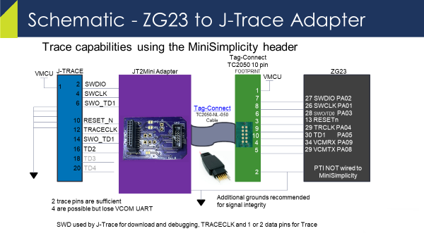
The SeggerJ-Trace Pro Cortex-M is required for Trace Debugging. While not, cheap, it’s also not expensive compared to the cost of an engineer working for days trying to capture how their firmware dropped into the weeds. The J-Trace connects to your PCB via a 20 pin header that is 50mil on centers so it is quite small. However, I’ve come up with a small PCB that lets you use the standard 10 pin MiniSimplicity header for Trace.
etm_zwave Github Repo and J2Mini Adapter
Most Z-Wave IoT products have very small PCBs and no room for another 20 pin header even if it is 50mil. I came up with a simple way to use the existing 10 pin tag-connect/MiniSimplicity header for Trace and placed all the files in a public github called etm_zwave. You do have to connect a couple of extra pins from the ZG23 to the tag-connect/MiniSimplicity header. Replace the PTI pins with the trace clock and a second data pin – the first data pin is the SWO pin already on the header. This header is tiny and you need a way to program the ZG23 anway and this is the way to go. The PTI pins are not that useful as they are only used for radio packet tracing which Z-Wave uses standalone Zniffers instead of wiring multiple nodes to the Network Analyzer. For less than $30 you can build your own JT2Mini adapter boards and then be able to use trace with just the MiniSimplicity header. You will need a extra ground connection as there is a single ground pin on the MiniSimplicity header. I’ll discuss that issue more in the troubleshooting section below.
JT2Mini adapter board plugs directly into the Segger J-Trace and MiniSimplicity cable. It only provides two trace data pins which Segger claims will only occasionally cause the CPU to stall. With 4 pins the CPU will almost never stall. Obviously with only 1 data pin you’ve cut the data rate to get the trace info out of the chip and it will stall (insert wait states) anytime the TPIU fifos will up until they are able to unload the data off-chip.
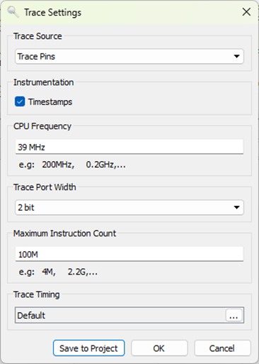
Setup Trace in Ozone
Now that the hardware is wired up, we have to enable Trace in Ozone.
Open Ozone
Include the *.JlinkScript file in the etm_zwave github repo
For the ZG23 use ZG23_Traceconfig.JLinkScript
There are comments in the file and more info in the repo ReadMe.md on how to properly insert the script into your Ozone *.jdebug project file.
Click on Tools->Trace Settings
Change the Trace Source to Trace Pins
CPU Frequency=39MHz
Trace Port Width=2 (if using JT2Mini)
Click on Green Power button
Ozone will download the code and run to MAIN()
Open the Timeline and Code Profile windows
The TimeLine should look something like this – maybe “run” for just a fraction of a second:
This window shows how long the CPU has been in each function and the complete program flow in real time. Interrupts and switching RToS tasks are shown and make it much easier to immediately find where the hardfault occurred. Clicking in the timeline brings up the exact line of C code and optionally disassembly at that instant in time. You can quickly follow exactly where your code went wrong and the hardfault occurred.
The Timeline window also allows you to immediately see how long each function is taking. What is most important here is checking your interrupt service routines to ensure they are not busy burning a lot of CPU time doing less important work and starving other time sensitive functions. The obvious waster of time is the memset and memcpy functions which I am working on another post about those specific functions so stay tuned!
Ozone has a Code Coverage window which displays the number of lines of code that have been executed and the number of assembly instructions executed. Using this feature with a product validation suite you can quickly identify untested and potentially dead code.
Segger has plenty of training videos that go into a great deal of detail on how to use these tools. But first you need a J-Trace and get it wired up to your board.
How to get printfs via J-Trace
Unfortunately the Segger J-Trace Pro does not support the VCOM serial interface. Thus, if you want to open a terminal window and see the printfs in your code, you have to jumper the Rx/Tx pins (and ground) to a Serial to USB adapter. Fortunately I put a header on the JT2Mini PCB for exactly this purpose. The J5 header has the Rx (Pin 1 square pad) and Tx pins on it (Pin 2 round pad). J3 has ground on both pins. Use an FTDI serial to USB adapter and PuTTY or other serial terminal program to view the printfs. The DevKit EXP pins should be able to read in the serial data but I was not able to find the right combination of In/Out/MCU and AEM/Bat/USB and get SSv5 to work. Thus I recommend using a simple FTDI interface to watch the printfs when tracing.
Troubleshooting
The number one challenge with getting Trace to work is the signal integrity of the clock and the trace data pins. Once you have a clean connection, it seems to be rock stable and produces really valuable debugging data even with just two data pins. If Ozone if giving strange errors and specifically different errors with each run, odds are you have a signal integrity problem.
Yellow is Trace Data1, Green is TRACECLK – GPIOs are at max bandwidth
The EFR32 Series 2 (including the ZG23) GPIOs have only a 20MHz bandwidth. The Trace clock is a divide by 2 of the 39MHz CPU clock so it is running right at the maximum of the GPIO. Trace data is clocked out on both edges of the clock. Since the MiniSimplicity header has only 1 ground on it and there are at least 3 GPIOs toggling at their maximum rates, the signal integrity is marginal even in the best of circumstances. The JT2Mini has extra ground pins and I highly recommend connecting them with additional jumper wire while using Trace. The cable from your board to the JT2Mini should also be no more than 6 inches long. The .JlinkScript file has code in it for adjusting the slew rate of the GPIOs which can improve or possibly degrade the trace signal integrity. Ozone and J-Trace can also adjust the relative timing of the CLK to the data with sub-nanosecond resolution. You’ll have to experiment on your own if you are having problems.
Conclusion
I can’t live without Trace debugging. I don’t necessarily use it all the time but I will wire it up to every board I design in the future! I have spent weeks debugging hardfaults in the past and then solve the problem in 10 minutes using Trace. Get one for yourself!
See many of you next week at the Z-Wave Summit in Orlando Florida where I will be giving a presentation on The Joys of Trace Debugging and running the UnPlugFest on Monday!
The two Z-Wave 800 series chips from Silicon Labs have flexible GPIOs but figuring out which one is the best for which function can be challenging. There are a number of restrictions based on the function and the energy (sleep) mode you need the GPIO to operate in. Similar to my posting on the 700 series, this post will guide you to make wise decisions on which pin to use for which function.
The tables below are a compilation of several reference documents but all of the data here was manually copied out of the documents and I could have made a mistake or two. Please post a comment if you see something wrong and I’ll fix it right away.
The table below lists the pins from the most flexible to the most fixed function. There are more alternate functions than the ones listed in this table. The most commonly used alternate functions are listed here to keep the table readable. Refer to the schematics and datasheets for more details.
Port A and B are operational down to EM2, other GPIOs will retain their state but will not switch or pass inputs. Thus, use port A and B for anything special and use C and D for simple things not needed when sleeping (LEDs, enables, etc).
WSTK GPIO Probe Points
Only the ZG23 QFN48 pin numbers are listed in the table. The QFN48 is expected to be pin compatible with future version of the ZG23 with additional Flash/RAM so I recommend using it over the QFN40. The WSTK2 is the Pro DevKit board with the LCD on it which comes as part of the PK800 kit. There are two sets of holes labeled with Pxx numbers on them which are handy to probe with an oscilloscope. The Thunderboard Z-Wave (TBZ) also has 2 rows of holes which are ideal for probing or connecting to external devices for rapid prototyping.
Name
ZG23
ZGM230
WSTK2
TBZ
ALT FUNC
Comments
PB2
22
9
P19
EXP5 BTN1
Use the pins at the top of this list first as they are the most flexible
PB6
NA
5
EXP15 I2CSDA
TBZ Qwiic I2C_SDA
PB5
NA
6
EXP16 I2CSCL
TBZ Qwiic I2C_SCL
PB4
NA
7
PA10
35
23
PC1
2
35
P1
EXP4
PC and PD are static in EM2/3
PC2
3
36
P3
EXP6
PC3
4
37
P5
EXP8
PC4
5
38
P35
BLUE
PC6
7
40
P33
EXP9
PC8
9
42
P31
LED0
PC9
10
43
P37
LED1
PD3
45
30
P26
IMUEN
PB0
24
11
P15
VDAC0CH0
PA0
25
12
P2
GREEN
IDACVREF
PB1
23
10
P17
RED
EM4WU3 VDAC0CH1
EM4WUx pins can wake up from EM4 sleep mode on a transition of the GPIO
PB3
21
8
P21
EXP3 BTN0
EM4WU4
PC0
1
34
P7
EXP10
EM4WU6
PC5
6
39
P12
EXP7
EM4WU7
PC7
8
41
P13
SNSEN
EM4WU8
PD2
46
31
P6
EXP11
EM4WU9
PD0_LFXTAL_O
48
33
XC32
XC32
BRD4210 and TBZ have 32KHz crystal mounted
PD1_LFXTAL_I
47
32
XC32
XC32
Accurate timing while sleeping – Time CC
PA7
32
20
P10
TraceD3
Trace pins for debug & code coverage
PA6
31
19
P8
TraceD2
Trace is configurable for 4, 2 or 1 data pin
PA5
30
17
P4
IMUINT
EM4WU0 TraceD1
PA4_TDI
29
16
P41
EXP13
JTAG_TDI TraceCLK
JTAG data in Trace Clock out
Pins below here should be used primarily for debug
PD4_PTIDATA
44
29
P25
Packet Trace Interface (PTI) data
PD5_PTISYNC
43
28
P24
EM4WU10
PTI Sync
PA9_URX
34
22
P11
EXP14
VCOM UART
PA8_UTX
33
21
P9
EXP12
VCOM UART
PA3_SWO
28
15
P16
JTAG_TDO TraceD0
RTT UART printf and Trace D0
PA2_SWDIO
27
14
P18
JTAG_TMS
These two SWD pins should ONLY be used for debug and programming
PA1_SWCLK
26
13
P20
JTAG_TCK
SWD debug clock
Pins below here are fixed function only
SUBG_O1
18
NA
Not used by Z-Wave
SUBG_I1
16
NA
Not used by Z-Wave
SUBG_O0
19
3
RFIO on ZGM230
SUBG_I0
17
NA
Matching network to SMA
RESET_N
13
1
F4
Push buttons on DevKit boards
HFXTAL_O
12
NA
39MHz crystal
HFXTAL_I
11
NA
39MHz crystal
DECOUPLE
36
18
1.0uF X8L cap (unconnected on ZGM230)
VREGSW
37
NA
Inductor to DVDD for DCDC – 3.3V
VREGVDD
38
25
3.3V In/Out based on mode
DVDD
40
24
VDCDC on ZGM230
AVDD
41
NA
Highest voltage – typically battery voltage
IOVDD
42
26
1.8-3.8V
PAVDD
20
NA
3.3V for +20, 1.8V for +14dBm
RFVDD
14
NA
1.8V or 3.3V but less than PAVDD
VREGVSS
39
27, 44
GND
RFVSS
15
2, 4
GND
Power Supply Pins
Obviously the power supply pins are fixed function pins. The only really configurable parts to this set of pins is the voltage to apply to the IOVDD, AVDD and whether to use the on-chip DC to DC converter or not. If your device is battery powered, AVDD should be the battery voltage assuming the battery is nominally 3V (coin cells or CR123A). AVDD can be measured by the IADC in a divide by 4 mode to give an accurate voltage reading of the battery. This avoids using GPIOs and resistor dividers to measure the battery level thereby freeing up GPIOs and reducing battery drain. IOVDD should be set to whatever voltage needed by other chips on the board. Typically either 1.8 or 3.3V. The DCDC should be used in most battery powered applications unless a larger DCDC is present on the board already to power other chips.
The other configurable voltage is the RFVDD and PAVDD and the choice there depends on the radio Transmit Power you wish to use. For +14dBm PA an RF VDD are typically 1.8V. For +20dBm PAVDD must be 3.3V.
Every product has unique requirements and sources of power so I can’t enumerate all possible combinations here but follow the recommendations in the datasheets carefully. Copy the radio board or Thunderboard example schematics for most typical applications.
Debug, PTI and Trace Pins
The two Serial Wire Debug (SWD) pins (SWCLK and SWDIO) are necessary to program the chip FLASH and are the minimum required to be able to debug firmware. While it is possible to use these pins for other simple purposes like LEDs, it is best if they are used exclusively for programming/debug. These should be connected to a MiniSimplicity or other debug header.
The SWO debug pin is the next most valuable pin which can be used for debug printfs in the firmware and output to a debugging terminal. Alternatively, the UART TX and RX pins can also be used for debugging with both simple printfs and able to control the firmware using the receive side of the UART to send commands.
The two Packet Trace Interface (PTI) pins provide a “sniffer” feature for the radio. These pins are read by Simplicity Studios Network Analyzer to give a detailed view of all traffic both out of and into the radio. The main advantage of these pins is that they are exactly the received data by the radio. The Z-Wave Zniffer can also be used as a standalone sniffer thereby freeing these pins for any use. The standalone Zniffer however does not show you exactly the same traffic that the PTI pins do especially in noisy or marginal RF conditions. Thus, the PTI pins on the device provide a more accurate view of the traffic to the device under test.
The Trace pins provide additional levels of debug using the Segger J-Trace tool. These pins output compressed data that the debugger can interpret to track the exact program flow of a running program in real time. This level of debug is invaluable for debugging exceptions, interrupts, multi-tasking RTOS threads as well as tracking code coverage to ensure all firmware has been tested. Often these pins are used for other purposes that would not be necessary during firmware debug and testing. Typically LEDs or push buttons can be bypassed during trace debug. There are options to use either 4, 2 or even 1 trace data pin but each reduction in pins cuts the bandwidth and make debugging less reliable.
LFXO and EM4WU Pins
The Low Frequency Crystal Oscillator (LFXO) pins are typically connected to a 32KHz crystal to enable accurate time keeping within several seconds per day. If supporting the Time Command Class, I strongly suggest adding the 32KHz crystal. While you can rely on the LFRCO for time keeping, it can drift by as much as a minute per hour. While you can constantly get updated accurate time from the Hub every now and then, that wastes Z-Wave bandwidth and battery power. Both the Thunderboard and BRD4210 include a 32KHz crystal so you can easily compare the accuracy of each method.
Reserve the EM4WU pins for functions that need to wake the EFR32 from EM4 sleep mode. These are the ONLY pins that can wake from EM4! Note that ports PC and PD are NOT able to switch or input from peripherals while in EM2. See the datasheet and reference manual for more details.
Remaining GPIOs
Many of the remaining GPIOs have alternate functions too numerous for me to mention here. Refer to the datasheet for more details. Most GPIOs can have any of the digital functions routed to them via the PRS. Thus, I2C, SPI, UARTs, Timers and Counters can generally be connected to almost any GPIO but there are some limitations. Analog functions have some flexibility via the ABUS but certain pins are reserved for special functions. Hopefully these tables help you make wise choices about which pin to use for which function on your next Z-Wave product.
Here we go again… Once again I’ve been given yet another board with randomly placed test points instead of a nice neat, reliable header to connect via my MiniSimplicity cable. So I’m spending an hour on my microscope soldering thin little wires to the tiny little test points to be able to flash and then debug the firmware on a new ZG23 based product. Once I’m done soldering, I’m left with a very fragile board which is unreliable at best and at worst will result in even less hair on my thinning head. My post from 2019 described using a zero cost header for a reliable connection, but it seems not everyone is reading my blog!
On the flip side, a different customer sent me their board with a Tag-ConnectEdge-Connect that I had not seen before but is absolutely brilliant. The Edge-Connect uses the EDGE of your PCB for the test points. Barely 1mm wide and about 20mm long it is possible to include this debug connector on virtually any PCB. There is a locking pin to hold the cable secure while the spring loaded tabs press into the castellated notches to ensure solid contact.
Close up of the locking pin and castellated notches
There are several sizes of the Edge-Connect but the recommended one is the 10-pin EC10-IDC-050 which matches the MiniSimplicity header on the WSTK DevKit board. Note that the the 6pin cable in the photo above is NOT the one I would recommend but it was the only one in stock at the time and it worked fine for debugging but doesn’t have the UART or PTI pins.
Tag-Connect has many other types of debug headers/cables of various configurations to hold the cable to the PCB securely. The original Tag-Connect cables have plastic clips that snap into fairly large thru-holes in your PCB. While this is a reliable connection, the thru-holes eat up a lot of PCB real estate. The next evolution was to use a small retaining clip under the PCB that grips onto the metal alignment pins. The photo below shows the PCB pads are not much bigger than an 0805 footprint and only requires three small thru-holes.
Note the smallest header is about the same as an 0805 in lower left corner
The lowest cost approach is to simply add a 10-pin header footprint on your PCB that matches the pinout of the MiniSimplicity header. See section 5.1.1 of Application Node AN958 for the pinout of the 10-pin MiniSimplicity header. You don’t need to solder the header onto the PCB except when debugging. Thus the header can be under a battery or some relatively inaccessible location as when you are debugging in the lab the PCB is usually not installed in the product enclosure.
Please use ANY of these standard connectors on your next project. Without a solid connection between your computer and the chip you will find yourself chasing ghosts and losing hair.
The Jasco Motion Dimmer is an ideal Z-Wave product for home automation. We want the lights to come on automatically when we enter a room and off again when everyone has left. The motion sensing needs to be reliable and sensitive and ideally not involve changing batteries every few months. Thus, a wall mounted, always-on dimmer with a built-in motion sensor fits our needs perfectly. In this blog article I’ll explain a few tricks to getting the most out of this handy device.
Configuration Parameters
The Jasco Motion Dimmer has 18 configuration parameters. The parameters can be set by reading the documentation and then programming them using complex combinations of button presses. But, with a Z-Wave device, it’s much easier to program them via Z-Wave. Most Hubs allow you to program the configuration parameters though the process to do so is different with every Hub. The parameters are briefly described on the Jasco web site ezzwave and on the Z-Wave Alliance web site. However, these brief descriptions don’t clearly describe what the parameter does and more importantly, what the best settings are to get the most out of this device.
Several parameters are two bytes instead of just one even though the value will typically fit in one (the value is 0-255). The parameters listed with a (2) in the Name field below means they are two bytes. If there is no (2) in the name then just send one byte. Sending just one byte to the 2 byte parameters can confuse the dimmer and it may not set the parameter to the desired value. The result is frustration as you sent it your desired value but it didn’t take it or set it to what appears to be some random value. Always send the proper number of bytes for each specific parameter. Some Hubs will handle this for you, but others must be done manually.
The table below is the list of all parameters with the less important ones greyed out and my own more detailed description of what each parameter does.
#
Name
Default
Description
1
Timeout
5
Motion Sensor Timeout 0=5s test mode 1-254=minutes 255=disable Time the lights remain on in Occupancy mode
2
Assoc dim
255
0=99 dim level 255=last ON level Dim level to send to associated lights. The Hub is better at controlling other lights so ignore this parameter.
3
Mode
3
1=Manual – Motion sensor does not control the local load 2=Vacancy – only turns lights off 3=Occupancy – Lights on when motion detected and off when none after Timeout
4
Invert buttons
0
0=normal (top=up, bottom=down) 1=invert (top=down, bottom=up) If you accidentally install the dimmer upside down, inverting it will correct your mistake
6
Motion Enable
1
0=disable 1=enable Why would you disable motion sensing?
7
Steps via Z-Wave
1
Leave at 1 See the Ramp Rate discussion below
8
Speed via Z-Wave (2)
3
Number of seconds for the dimmer to go from 0 to 100% via a Z-Wave command
9
Steps via button
1
Leave at 1
10
Speed via button (2)
3
Number of seconds for the dimmer to go from 0 to 100% via a button press or the motion sensor
11
Steps via AllOnOff
1
AllOnOff commands are obsolete
12
Speed via AllOnOff (2)
3
Leave at default
13
Motion Sensitivity
2
1=high – detects people at a distance 2=Medium 3=low – less likely to detect a pet
14
Light Sensing
0
0=disabled 1=enabled If enabled and the room is brightly lit the lights will not turn on when motion is detected
15
Reset Time (2)
2
0=disabled 1=10s, 2=20s, 3=30s, 4=45s, 5-255=n*15s When Motion is detected a notification is sent to the hub saying there is motion. After Reset Time, a reset notification to clear the motion event is sent. If you are still in the room, motion and reset notifications will continue to be sent. Depending on your hub you may want to change this but generally the default works.
16
Switch Mode
0
0=disabled 1=enabled Switch mode changes the dimmer to act like a switch so the light turns on (100%) or off instantly. If you want this mode, buy the cheaper switch instead.
17
Switch Level
0
0-99=Brightness level Sets the dim level when motion is detected or the top button is tapped. You can press and hold the top which will continue to increase the dim level further if you have set this to something other than 99. Ignored when Switch Mode is enabled.
18
Dim Up rate
0
0=fast 1=slow This applies only to commands sent via Z-Wave and only applies to the dim up ramp rate. Best to leave this at the default of 0 and use parameters 8 and 10 instead.
19
Exclusion Mode
0
0=any button 1=Tap X then ON will enter exclusion mode, Tap X then tap OFF 10 times in less than 5 seconds will factory reset the dimmer. X is the little button behind the face plate to the left of the ON button. Enable this mode if there are other Z-Wave networks nearby (IE: in a condo or apartment) to reduce the risk that one of these other networks will exclude the dimmer when you tap one of the buttons. When 0, every time you tap either On or Off the NIF is sent. If a nearby controller is in exclusion mode, your dimmer will be excluded from YOUR network and it will seem to stop working. I recommend setting this to 1 either way to reduce the chance even within your own household of accidentally excluding the dimmer.
Configuration Parameters
Dimming Ramp Rates
When a dimmer changes the light level from 0 to 100%, the time it takes for the light to go from 0 to 100% is set by the Ramp Rate. The dimmer has six parameters related to the dimming ramp rate, parameters 7 through 12. The ramp rate is configured using a pair of parameters for three different methods of changing the light level. The “Steps or Levels” is the number of dim levels that the light level changes every Time Step. Always leave the Steps at the default of one. Anything more than one results in the light level “jumping” from one step to the next while dimming. This jumping is just plain unpleasant so always leave Steps at one. The Time Step parameter (Speed) is how often the Step is added to the current dim level in 10 millisecond increments or every 1/100th of a second. Since the dim level goes from 0 to 100 and it takes 1/100th of a second to increment once, then the Time Step simply is the number of seconds for the dim level to go from 0 to 100%. The default ramp rate is three seconds which is what most people expect and in general is a good value.
The three pairs of ramp rates provide different ramp rates based on the method to turn the light on or off.
Z-Wave command – parameters 7 and 8
Button or Motion detection – parameters 9 and 10
All On/Off commands – parameters 11 and 12
The easy ones to ignore are the All On/Off parameters as the Z-Wave All On/Off commands are obsolete. Simply leave these at the default. The remaining two pairs can be used for different purposes based on what is changing the light level. I recommend leaving the Button/Motion parameters at the default of 3 seconds. This is the expected ramp rate of the average dimmer. When a person presses the button or motion is detected, they expect the dimmer to react at about this speed. Setting it to less than 3 seconds results in the user being unable to set a mid-level as the ramp rate is too fast to accurately stop at a mid level. The dimmer pretty much becomes a switch. Setting the ramp rate to more than 3 seconds will quickly become annoying as it just takes too long to get to the desired level. That leaves the Z-Wave command ramp rate parameters. These can definitely be programmed to be longer, potentially much longer so that the level changes quite slowly and an occupant can override the slowly changing light level by pressing the button or waving their hands in the air so the motion sensor will detect them.
The Z-Wave Multilevel Switch command Version 2 includes a Duration field which is the number of seconds to go from 0 to 100% or the ramp rate. If the Hub sends a dim level command with the Duration field, the configuration parameters are ignored and instead the ramp rate is set to the Duration value in the command. Some Hubs let you assign the Duration field but most only support Version 1 which only has the level and no duration which the dimmer will then use the configuration parameters dim rate.
Association Groups
Three association groups are supported with up to five NodeIDs each. Your Hub should automatically assign itself to Group 1 which is the Lifeline group. The Lifeline group is required for every Z-Wave Plus device and identifies the NodeID where any state changes will be sent. The dimmer sends your Hub commands whenever the sensor detects motion or the state of the local load changes (someone presses the On or Off button). Thus, it is very important that the Hub be assigned to Association Group 1 so Hub app on your phone matches the actual state of the dimmer.
Groups 2 and 3 are identical and simply send Basic On/Off commands to the associated NodeID. Assigning a NodeID to these groups will send a command to turn the NodeID either On or Off when motion is detected or not. Assigning a NodeID to these groups enables the motion detector or the buttons to turn on/off other lights in a larger room quickly. Using the association groups is fast since the dimmer sends the Z-Wave commands directly to the light and works even if the Hub is offline for some reason.
Multi-channel associations are supported but generally you want to avoid them. Multi-channel adds another layer of encapsulation to every frame which just slows everything down. The only time you might want to use multi-channel association is if you wanted to control a specific outlet in a power strip with the motion sensor. Multichannel would be required to choose which of the outlets in the power strip to turn on/off. However, I recommend that you let your Hub do complex operations like this and keep things simple with the dimmer.
Group
Name
Description
1
Lifeline
Motion Sensor readings and status of the load are reported
2
Basic On/Off
BASIC SET On or Off commands
3
Basic On/Off
BASIC SET On or Off commands
Association Groups
When a NodeID is assigned to an association group, the node will be interviewed and depending on the command classes the node supports, the dimmer will send different commands. Specifically, if the device supports CRC16 then the commands will be encapsulated in CRC16 which improves the reliability of the command being delivered without errors but isn’t really necessary.
Why are there two association groups you ask? The reason is to match the feature set of many other Jasco Z-Wave products which send different commands in the two groups. But for this device it always sends the same commands from either group. My recommendation is to not use Group 3 at all. If you want to associate other lights directly with the dimmer, use Group 2.
Recommendations
There are many ways to use a motion sensor wall dimmer. Perhaps the toughest question is where to install it? The first place I installed my motion dimmers are in hallways. When your arms are full of groceries, you want the lights to just come on when you enter. More important in my household is that the lights go OFF shortly after everyone has left the hallway! Back in the bad ol’ days, the hallway lights were always on all the time because no one ever turned them off! The challenge with hallways is typically they are 2, 3 or more way lights so the placement of the motion sensor is key. Jasco makes an inexpensive Add-On Switch that connects to the Traveler wire to enable the multi-way switch so it can be operated manually as before. However, getting the motion sensor to cover a long thin hallway can be difficult since the motion sensor is built into the wall and cannot be pointed down the hallway. In that case you may need to use a separate battery powered motion sensor to trigger normal dimmer switches. What this means is that a wall mounted fixed position motion sensor may not work for all situations but the sensor has a wide angle lens so it will work most of the time.
Easy Mode – Use the Defaults
The simplest configuration is to use the dimmer as-is using the default settings. The defaults work as you would expect and obviously is the easiest to setup and use! Perhaps the only real decision here is which wall switch to replace. In this mode the lights come on when motion is detected and off after 10 minutes. Perhaps the one configuration to adjust would be the Timeout especially for hallways. Since you’re usually passing thru the hallway and thus moving quite a bit, the Timeout can be short, one or two minutes. A short Timeout keeps the power consumption to a minimum while providing sufficient light to travel thru the space.
Slow Dim – Parameter 8
The next parameter to consider customizing is the Z-Wave dim ramp rate (Parameter 8). The motion sensor and the buttons continue to use the typical 3 second ramp rates which are what people would normally expect. But when a Z-Wave command sends a command to change the light level, a significantly slower ramp level can be used. This configuration lets the user override the dim level either by moving or pressing a button. The slow ramp can be 30 seconds in this mode or perhaps as short as 10s. This always gives the person in the room time to override the slow dim but still provide enough light to move around the room as needed. The most common case for this is in a room where people might be reading, watching TV or working on a computer where they are not moving very much.
Manual Mode – Parameter 3
Configuration Parameter 3 has three different settings. The default is Occupancy mode which is the most useful and common mode. Vacancy mode only turns the light off but you have to manually turn it on – don’t bother with this mode. The third option is Manual mode which disconnects the motion sensor from the local load. Your Hub has to then turn the light on when the motion sensor detects motion. The time from motion detection to the light coming on has just a little more delay but often this delay isn’t that much. What you gain from this setup is a great deal more flexibility in how the lights should dim up or down.
My Setup
The first motion dimmer I installed was in my mudroom which is pretty much a hallway with a closet but it is an L shape. It is a 3-way switch with wall switches at each of the 3 entrances. Fortunately the switch with the incoming power is the one with the best view down both legs of the L and is where I mounted the motion dimmer. I use Easy Mode in this situation since the desired operation is quite simple. You walk in, the lights come on, you leave and 10 minutes later the lights go off. I suppose I should shorten the Timeout but I’ve never been in the mudroom and had to waive my hands to turn them back on even when rummaging thru the closet where the motion sensor can’t really see me. If I made the timeout shorter, then the lights might go off before I’ve found what I’m looking for. Nothing craters the WAF Factor more than the lights turning off before my wife has found what she’s looking for in the closet!
The next one I installed is in the garage. In this case I used a Motion Switch rather than a Dimmer since its a few bucks cheaper and I don’t need a dimmer in the garage. Easy Mode is fine in this situation. I have a 2 car garage about 24′ square and the motion sensor is able to detect motion of a person just about anywhere in the room even though the wall switch is in the corner next to the door into the mudroom. I did change Motion Sensitivity (Parameter 13) to high to get the entire garage to detect motion. I also enabled Light Sensing (Parameter 14) as my garage has quite a few windows and has plenty of light during the day. There is no way to adjust the level of light to disable the light from turning on but it seems to work when I want it to and doesn’t turn on the lights when the room is sufficiently bright from natural sunlight.
My master bedroom closet seemed like a simple setup but took a little more tweaking. What I want is the light to come on at a low level (say 5%) but if it’s daytime or early evening I want the light to come on fully. With this setup the light is just enough to find my robe in the middle of the night without waking my wife but she can choose an outfit in full illumination. Since the dimmer has no idea what time of day it is, I need to enlist the help of my hub. I set the Switch Level (Parameter 17) to 5% and the Z-Wave Dim Rate (Parameter 8) to 30 seconds. Then I created an event on my hub (Homeseer) that sends an ON command whenever motion is detected and the time is between sunrise and 9pm. This ON command will take 30s to come on fully which is nice. Since the Button Dim rate remains at 3s the buttons operate as normal so if my wife is impatient she can press the top button to quickly get the lights fully on.
My kitchen is the most complicated setup by far. First of all, I have an eat-in kitchen which is pretty wide and the dimmer often doesn’t detect if we are sitting at the table which is at the end of the kitchen. The Jasco Motion sensor is mounted basically in the middle of my kitchen and there are a variety of kitchen appliances on the counter blocking the view of the kitchen table. To cover this wide space I enlist a second motion sensor that is close to the table so even if someone is sitting there quietly, perhaps reading, the combination of the two sensors ensures that the lights only go off when no one is there (most of the time). I use Manual Mode (Parameter 3) in this case and rely on my Hub to combine the 2 sensors readings and control the lights appropriately. Manual Mode effectively disconnects the Jasco Motion Sensor from the Dimmer. When either motion sensor detects motion, I set the dimmer to full on. When BOTH motion sensors have not detected motion for about 20 minutes, then I turn the dimmer off. By relying on the smarts of my Hub I can do even more interesting events where the timeout is different late at night when someone is probably just passing thru and I can use a lower dimmer level. At meal times I push the dimmer fully on as we’re probably preparing food so the more light the better. I could even check for the light level provided by the windows in the room and then only add as much illumination as needed though I haven’t experimented with this yet.
Conclusion
Once you have a few lights automated, you’ll almost never touch the buttons. The lights come on when you walk in and off when everyone leaves. Your family quickly becomes used to it and it blends into the woodwork which is the way things should work. Adding motion sensor lights to your home is an incremental upgrade. I suggest starting with your most-used light such as a hallway or mudroom. Once the family has adjusted to one, you can add more in other locations as the budget allows.
The Jasco Motion Dimmer is a versatile and invaluable home automation device. Never needs batteries and is configurable enough to handle even fairly complicated situations. The trick is to use the right tool for the job. The dimmer is fine for basic operation but use the smarts built into your Hub to do more complicated tasks. Being highly configurable unfortunately results in more complexity but I hope my guide helps you make the most of this device. Let me know what you think and any other Z-Wave related topics you’d like to discuss in the comments below.
You have a second MCU or other data files you want to update using Over-The-Air (OTA) via Z-Wave. How can you reuse the Bootloader firmware to verify the signature and decrypt the data?
The code to verify and decrypt the file already exists in the bootloader and is known good. Reusing the existing bootloader code is smaller and safer than re-inventing the wheel – or in this case encryption.
The attached project is a modified Z-Wave Door Lock Key Pad sample application that demonstrates how to OTA code/data other than the Z-Wave firmware. OTA of the Z-Wave firmware works in the sample application already – but first the encryption keys MUST be generated. See https://www.silabs.com/community/wireless/z-wave/knowledge-base.entry.html/2019/04/09/z-wave_700_ota_ofe-i00M on how to generate the keys. See the two .BAT files in the comments section which will run all the necessary commands for you. They are also included in this .sls file in the KEYS directory. You MUST create your own project keys to OTA either the Z-Wave Firmware or any other data.
To OTA other types of files you need to start with a binary file. Most microprocessor development environments will output a binary file so use that instead of a HEX file. If you have an Intel hex or Mototola S record file, use a utility like SREC_CAT to convert it to a binary file. SREC_CATcan convert just about any file type into any other file type. If the file is more than 200K bytes, you will need to break the file into 200K or smaller files and OTA each, one at a time. Doing that is beyond the scope of this project. Note there is no need to encrypt the file. We will be using Commander to sign and encrypt it using the keys generated here.
Theory of Operation:
Changes to the SSv4 DoorlockKeyPad sample project are indicated with the comment “AKER” – search for these to find what changed. You can also diff the files with a fresh copy of the DoorLockKeyPad sample app from SSv4. Most of the code to support OTA of an external processor is in this file. A few changes have been made to ota_util.c in ZAF_CommandClasses_FirmwareUpdate but these are expected to be included in a future release of the SDK (currently tested on 7.13).
Commander is used to generate a pair of public and private keys. The private key is then programmed into every device to be OTAed. Commander then encrypts and signs the binary file and wraps it with bootloader tokens. The gbl file is downloaded, the signature checked and the encrypted data is then passed to a callback function 64 bytes at a time. You then have to store the data or pass it to the external MCU. This example simply prints the data out a UART.
Procedure:
Step 1: Generate the keys
There two .BAT files in the KEYS directory for this project. These are windows script files. For other platforms you can easily convert them to the platform specific commands. See the comments in the files for more details. In a windows shell type: GenGblToken.bat This will use Commander to generate a project set of keys in the files vendor_*.*. Only execute this command ONCE. The same keys are used for the duration of the project. If you change the keys then you cannot OTA the devices as the keys no longer match.
Step 2: Program the key into a devkit and every DUT
Each device manufactured must have the private key programmed into FLASH. Use the PgmToken.bat to program the key into a target device connected via USB. Note that EVERY unit manufactured must have these keys programmed into it.
Step 3: Generate the .gbl file
Create the .gbl file from the binary file using the following command: commander gbl create <OTA_FileName>.gbl –metadata <BinaryFile> –sign vendor_sign.key –encrypt vendor_encrypt.key The –metadata option will wrap the binary data with the necessary tokens for the bootloader to parse the data. Do not use the –compress option. If the data needs to be compressed, use your own algorithm for that. There are 3 sample binary files in the KEYS directory – a small .WAV audio file, a large .M4A audio file and a PNG image file. Use the command above to wrap the file with the necessary tokens for OTA.
Step 4: OTA the .gbl file
Use the PC Controller or other application to send the gbl file over Z-Wave. Once the entire file has been sent and the CRC checked to be good, the FinishFwUpdate function is called to begin processing the image. Note that in the PCC you have to first GET the Current Firmware, then select the Target: 1 to download the metadata. Then click on UPDATE and the OTA will begin. Connect a terminal to the VCOM port of the WSTK to view the data streaming down during the OTA. Once all the data is sent down, the signature is checked and the decrypted data is sent out the UART. This is where you would need to change the code to store the data instead of printing it out the UART.
Step 5: Verify the Signature and pass in the callback function
The bootloader_verifyImage() function is called and the metadataCallback function is passed in. bootloader_verifyImage first returns a zero if the signature matches. If the signature fails an error value is returned giving some details on why it failed. The time to verify the signature can be fairly long depending on the size of the image so the watchdog timer is disabled during the processing.
Step 6: MetadataCallback passes blocks of 64 bytes of the decrypted data
The function passed in to bootloader_verifyImage is called with a pointer to the data and the number of bytes in each block. The size of the block can vary up to 64 bytes. In this example the data is simply printed out the UART. In your application you would replace this function with code to store the data as needed on the other MCU or external NVM.
Step 7: Reboot
It is recommended to reboot after the image data has been stored to ensure the FLASH is cleaned up properly. The current demo however does not reboot.
Note: This is an SSv4 SDK 7.13 sample but the same concepts should work in SSv5. The changes to ota_util.c will be folded into the SDK in a future release but for now those changes are necessary.
One of the challenges with using the Z-Wave developers kit is trying to figure out which pin is connected to what. Every pin of the ZGM130S can perform multiple functions but some pins are best used for certain things. This guide provides general recommendations, but these are not hard-and-fast rules. The ZGM130S provides a great deal of flexibility so feel free to explore the many options each pin and peripheral has to offer. I’m hoping I can guide you with some initial suggestions but feel free to delve into the details to find your ideal solution.
This guide is a compilation of a number of documents and while I’ve been thorough, I could easily have made a typo here or there. Please use the online documentation as the official reference and send me an email pointing out my error and I’ll fix it. I couldn’t possibly include every feature for every pin but the details are available in the reference documents below. The Decoder Ring below is an overview of the most commonly used features. The table below contains a lot of information, so you’ll need to view it on a computer with a big screen.
Reference Documents
ZGM130S ZGM130S Datasheet – See section 6 for the pin definitions EFR32XG13 Gecko Family Reference Manual – Each peripheral is detailed here UG381 ZGM130S Zen Gecko DevKit Users Guide – Section 3 describes connectors
ZGM130S GPIO Decoder Table
ZGM130S
GPIO port as described in the ZGM130S data sheet
Pin #
GPIO pin number of the ZGM130S SIP package
BRD4202A
Zen Gecko Developers kit board for the ZGM130S
BRD8029A
Button/LED board plugged into the WSTK EXP header for the sample apps
WSTK EXP
Pin number of the main WSTK board expansion header
WSTK
Main developers kit board with USB, LCD and Segger J-link debugger
The Pxx pins are the holes across the long side of the board
The Fxx pins are secondary functions that typically connect to the isolators
MiniDBG
Small 20 pin ribbon cable used to connect WSTK to a target DUT
ALT FUNCS
Alternate functions the GPIO can perform. All GPIOs can be simple digital 1/0s.
Some pins have special analog or peripheral functions.
Comments
Brief comments describing special functions of the GPIO
Description of the columns in the table below
General Purpose IOs – Use these for your application first
ZGM 130S
Pin #
BRD 4202A
BRD 8029A
WSTK EXP
WSTK
Mini DBG
ALT FUNCs
Comments
PD10
27
LED_R P201-35
P32
LED ON=low, Pullup Ideal for PWM
PD11
28
LED_G P201-37
P34
LED ON=low, Pullup
PD12
29
LED_B P200-3
P36
LED ON=low, Pullup
PC6
58
P201-4 P200-29
EXP4
P1 F16
Easy to use with WSTK since they are on EXP
PC7
59
P201-6
EXP6
P3
PF3
5
P201-13 P200-16
LED1
EXP13
P10
JTAG_TDI
PF4
6
P201-11 P200-23
LED0
EXP11
P8
PF6
8
P201-7 P200-25
BUTN0
EXP7
P4 F12
PC8
60
P201-8 P200-28
EXP8
P5 F15
PC9
61
P201-10
SW
EXP10
P7
PB14
46
P201-30
P27
LFXO – 32Khz osc crystal for accurate time
PB15
47
P201-32
P29
LFXO
PD9
26
P201-33
P30
PF5
7
P201-28 P200-24
P25 F11
PD13
30
P201-34 P200-31
P31 F18
OPA1P
Use for Analog functions
PD15
34
P201-38
P35
OPA1N
PA2
37
P201-3 P200-21
LED2
EXP3
P0 F8
OPA0P
PA4
39
P201-17
P14
OPA0N
PA5
40
P201-19 P200-18
P16 F5
VCOM_ENB Must be 1 for WSTK to pass USART0 to USB
Special Function Pins – Use these for their alternate function
ZGM 130S
Pin #
BRD 4202A
BRD 8029A
WSTK EXP
WSTK
Mini DBG
ALT FUNCs
Comments
PC10
62
P201-15
BUTN2
EXP15
P12
EM4WU12 I2C1_SDA
EM4WU pins are the ONLY pins that will wakeup from EM4
PC11
63
P201-16
BUTN3
EXP16
P13
I2C1_SCL
Use for I2C, will NOT wakeup from EM4
PD14
31
P201-36 P200-30
P33 F17
OPA1 EM4WU4
PF7
9
P201-9 P200-26
BUTN1
EXP9
P6 F13
EM4WU1
PA3
38
P201-5 P200-22
LED3
EXP5
P2 F9
VDAC0 OPA0 EM4WU8
PB11
41
P201-21 P200-34
P18 F21
OPA2P
PB12
42
P201-23 P200-33
P20 F20
10
OPA2
PTI_DATA Future Packet Trace debug
PB13
45
P201-25 P200-32
P22 F19
9
OPA2N EM4WU9
PTI_SYNC Always wire the 2 PTI pins on the ZG14 modem chip to GPIOs on your host CPU
Legend: WSTK = hole name (ZGM130 GPIO) EX: WSTK P100 pin 16 is hole P13, ZGM130S GPIO PC11, Button 3 on the BRD8029A BRD8029A is the Button/LED board. Functionality is: LEDs are ON when driven high BUTN pins are pulled up and go low when the button is pressed The SW can pull the pin either up or down depending on the slide setting left/on is 1, right/off is 0 thru 1MOhm resistors The VMCU powers the LEDs/Buttons but the board ID is powered via pin 20 Schematic is in Simplicity Studio
Mini-Simplicity Debug header: Top View
Name
Pin #
Pin #
Name
VAEM (3V3)
1
2
GND
RESET_N
3
4
VCOM_RX (PA1)
VCOM_TX (PA0)
5
6
SWO(PF2)
SWDIO(PF1)
7
8
SWCLK(PF0)
PTI_SYNC(PB13)
9
10
PTI_DATA(PB12)
On the DUT board with the ZGM130S on it, connect VCOM_RX to PA1 and VCOM_TX to PA0. The header is a 0.05” pitch 10 pin header. Typically use a Samtec FTSH-110 but to make the pads even smaller use just the pads for a thru-hole connector. See my post “700 series Debug Header” from October 2019 for more details on the debug header.
Recommendations
Remember that the GPIOs in all the Wireless Gecko chips from Silicon Labs are very flexible and most peripheral functions can be routed to almost any IO pin. That said, there are some pins that have fixed functions and some pins are best at certain other functions. Let’s start with the pins you can’t use.
Power Pins
Obviously, the power pins have to be connected to the proper voltage. The ZGM130 has a lot of ground pins so make sure every one of them is connected to a solid ground. The voltages for the power pins have a few rules but in most cases you’ll tie AVDD and VREGVDD to the same power source of 3.3V. The on-chip DC to DC regulator allows a wide voltage range on VREGVDD so there is some additional flexibility which requires careful consideration. But for most applications, tie these two power pins directly to the battery. Most of the time IOVDD is also tied to the battery though depending on other chips in your system you might need an LDO to keep the IOs at the proper voltage.
Debug Pins
The next set of pins you should not use for GPIOs are the debug pins. All ten IO pins on the Mini-Simplicity header should be wired up as shown in the table above. The UART pins are very important to print out debug information while the chip is running. The advantage here is that you can see things happening in real-time without using a scope or logic analyzer. And you can easily enable/disable blocks of debug statements as needed. The sample apps print all sorts of debug information so you’ll want to do the same in your code. The UART defaults to only 115200 baud but it’s easy to increase it up to roughly 1Mbaud to reduce the time impact of printing debug messages. Also, keep the messages short or else they may impact the timing so much that your code will fail. If you’re really in a pinch for one more IO, you could use the SWO or VCOM_RX pins as you probably don’t need them.
Special Function Pins
A number of pins have specific functions especially for certain analog functions. The ADC/DAC only have their primary and alternate IOs though you can route them thru the ABUS. Only a few of these pins can wake the chip from sleeping in EM4. Be very careful and utilize these pins for buttons or sensors that need to wake the chip up.
General Purpose IOs
The rest of the pins are available for any purpose. Most of the pins can be any digital IO function. Some pins are handy because of their connection on the DevKit. There are three IOs connected to an RGB LED on the 4202 board. These are really handy to visually observe PWM waveforms based on the color of the LED. The pins that are routed to the EXP header on the WSTK are easy to connect to a proto board. Be careful to avoid using PA5 as that is connected to the VCOM enable pin on the WSTK. PA5 has to be high to route the debug UART data to the USB bus. But this is a restriction only when using the DevKit 4202 board. If connecting to your own PCB via the Mini-Simplicity header you can freely use PA5.
Conclusion
The ZGM130S is a flexible chip with plenty of compute power, RAM and Flash. The GPIOs can largely be routed from any peripheral to any IO though there are some restrictions. The secret decoder ring given here maps out which pin can do what and which ones should be used for your application. This is only a guide and the chip has many more features than I can describe here. Refer to the Reference Documents for more in depth knowledge.
We’re all trying to make the Smart Home products smaller and less visible. Using coin cells instead of bulky cylindrical batteries significantly reduces the size of many products. The challenge with making products smaller is that the area available on the PCB for a debug header is in short supply.
With the 500 series I usually used a 0.1″ spacing 12 pin header from the ZDP03A programmer to the target board. The header was normally not installed in the final product but for debug purposes the solid thru-hole connector meant I would reliably program a device the first time and every time.
However, many customers I’ve worked with want to use less PCB real estate which means they come up with a custom set of test points. Typically a jig with spring loaded pins are used to contact to the PCB or more often wires are soldered to the PCB. The problem with this solution is that the jig is large, expensive and fragile. Soldering a cable to a board often results in a fragile connection where the cable can easily break a pin and not be immediately obvious. I’ve spent far too much time trying to figure out why I could program the part a minute ago but now I can’t only to realize the cable has a loose wire.
Unreliable Z-Wave programming cable
500 Series Header
My recommendation for the 500 series is to use a full size 12 pin 0.1″ spacing connector for programming and debug. Either SMT or thru-hole is fine but either way you have a solid, reliable, portable connection. While this worked OK with the 500 series which typically used large cylindrical batteries, the 700 series often uses coin cells which doesn’t have the real estate for a full size connector.
Reliable 500 series header = 15x5mm
700 Series Debug Header
Fortunately Silicon Labs has an even better solution for the 700 series – use a 0.05″ spacing 10 pin SMT header. The Mini Simplicity Debug connector is described in AN958. If you have a little room then use the standard SMT header which is 6x6mm. If you are very tight on real estate then put down the pads for the thru-hole version of the connector but hand-solder the thru-hole header to the pads. Using just the pads results in a header only 3x6mm. You can’t tell me you can’t come up with 18sqmm to make the PCB debug reliable!
Either solution requires only a small amount of space on a single side of the PCB. Usually the header pads can be under a coin cell since during debug a power supply is used instead of the battery. This same header can be used for production programming using a jig to contact to the pads. Having a standard and reliable connection to the PCB will save you time during debug and on the production floor.
Reliable 700 series header = 6x6mm
Conclusion
No matter how tempted you might be to come up with your own cable/connector/test points, DON’T DO IT! Use the standard Mini Simplicity connector to save you so many headaches during debug. A solid, reliable debug connection is an absolute must otherwise you risk spinning your wheels chasing ghosts that are caused by a flakey connector. Take it from me, I’ve tried to debug just way too many of these over the years and it is not fun.