The two Z-Wave 800 series chips from Silicon Labs have flexible GPIOs but figuring out which one is the best for which function can be challenging. There are a number of restrictions based on the function and the energy (sleep) mode you need the GPIO to operate in. Similar to my posting on the 700 series, this post will guide you to make wise decisions on which pin to use for which function.
The tables below are a compilation of several reference documents but all of the data here was manually copied out of the documents and I could have made a mistake or two. Please post a comment if you see something wrong and I’ll fix it right away.

Reference Documents
- EFR32xG23 Z-Wave 800 SoC Family Datasheet
- ZGM230 Z-Wave 800 Module Datasheet
- EFR32xG23 Reference Manual
- WSTK2 Schematic (available via Simplicity Studio)
- BRD4210 EFR32ZG23 Radio Board +20dBm Schematic
- Thunderboard Z-Wave UG532 and Schematic
Pin Definitions
The table below lists the pins from the most flexible to the most fixed function. There are more alternate functions than the ones listed in this table. The most commonly used alternate functions are listed here to keep the table readable. Refer to the schematics and datasheets for more details.
Port A and B are operational down to EM2, other GPIOs will retain their state but will not switch or pass inputs. Thus, use port A and B for anything special and use C and D for simple things not needed when sleeping (LEDs, enables, etc).
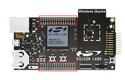
Only the ZG23 QFN48 pin numbers are listed in the table. The QFN48 is expected to be pin compatible with future version of the ZG23 with additional Flash/RAM so I recommend using it over the QFN40. The WSTK2 is the Pro DevKit board with the LCD on it which comes as part of the PK800 kit. There are two sets of holes labeled with Pxx numbers on them which are handy to probe with an oscilloscope. The Thunderboard Z-Wave (TBZ) also has 2 rows of holes which are ideal for probing or connecting to external devices for rapid prototyping.
| Name | ZG23 | ZGM230 | WSTK2 | TBZ | ALT FUNC | Comments |
| PB2 | 22 | 9 | P19 | EXP5 BTN1 | Use the pins at the top of this list first as they are the most flexible | |
| PB6 | NA | 5 | EXP15 I2CSDA | TBZ Qwiic I2C_SDA | ||
| PB5 | NA | 6 | EXP16 I2CSCL | TBZ Qwiic I2C_SCL | ||
| PB4 | NA | 7 | ||||
| PA10 | 35 | 23 | ||||
| PC1 | 2 | 35 | P1 | EXP4 | PC and PD are static in EM2/3 | |
| PC2 | 3 | 36 | P3 | EXP6 | ||
| PC3 | 4 | 37 | P5 | EXP8 | ||
| PC4 | 5 | 38 | P35 | BLUE | ||
| PC6 | 7 | 40 | P33 | EXP9 | ||
| PC8 | 9 | 42 | P31 | LED0 | ||
| PC9 | 10 | 43 | P37 | LED1 | ||
| PD3 | 45 | 30 | P26 | IMUEN | ||
| PB0 | 24 | 11 | P15 | VDAC0CH0 | ||
| PA0 | 25 | 12 | P2 | GREEN | IDACVREF | |
| PB1 | 23 | 10 | P17 | RED | EM4WU3 VDAC0CH1 | EM4WUx pins can wake up from EM4 sleep mode on a transition of the GPIO |
| PB3 | 21 | 8 | P21 | EXP3 BTN0 | EM4WU4 | |
| PC0 | 1 | 34 | P7 | EXP10 | EM4WU6 | |
| PC5 | 6 | 39 | P12 | EXP7 | EM4WU7 | |
| PC7 | 8 | 41 | P13 | SNSEN | EM4WU8 | |
| PD2 | 46 | 31 | P6 | EXP11 | EM4WU9 | |
| PD0_LFXTAL_O | 48 | 33 | XC32 | XC32 | BRD4210 and TBZ have 32KHz crystal mounted | |
| PD1_LFXTAL_I | 47 | 32 | XC32 | XC32 | Accurate timing while sleeping – Time CC | |
| PA7 | 32 | 20 | P10 | TraceD3 | Trace pins for debug & code coverage | |
| PA6 | 31 | 19 | P8 | TraceD2 | Trace is configurable for 4, 2 or 1 data pin | |
| PA5 | 30 | 17 | P4 | IMUINT | EM4WU0 TraceD1 | |
| PA4_TDI | 29 | 16 | P41 | EXP13 | JTAG_TDI TraceCLK | JTAG data in Trace Clock out |
| Pins below here should be used primarily for debug | ||||||
| PD4_PTIDATA | 44 | 29 | P25 | Packet Trace Interface (PTI) data | ||
| PD5_PTISYNC | 43 | 28 | P24 | EM4WU10 | PTI Sync | |
| PA9_URX | 34 | 22 | P11 | EXP14 | VCOM UART | |
| PA8_UTX | 33 | 21 | P9 | EXP12 | VCOM UART | |
| PA3_SWO | 28 | 15 | P16 | JTAG_TDO TraceD0 | RTT UART printf and Trace D0 | |
| PA2_SWDIO | 27 | 14 | P18 | JTAG_TMS | These two SWD pins should ONLY be used for debug and programming | |
| PA1_SWCLK | 26 | 13 | P20 | JTAG_TCK | SWD debug clock | |
| Pins below here are fixed function only | ||||||
| SUBG_O1 | 18 | NA | Not used by Z-Wave | |||
| SUBG_I1 | 16 | NA | Not used by Z-Wave | |||
| SUBG_O0 | 19 | 3 | RFIO on ZGM230 | |||
| SUBG_I0 | 17 | NA | Matching network to SMA | |||
| RESET_N | 13 | 1 | F4 | Push buttons on DevKit boards | ||
| HFXTAL_O | 12 | NA | 39MHz crystal | |||
| HFXTAL_I | 11 | NA | 39MHz crystal | |||
| DECOUPLE | 36 | 18 | 1.0uF X8L cap (unconnected on ZGM230) | |||
| VREGSW | 37 | NA | Inductor to DVDD for DCDC – 3.3V | |||
| VREGVDD | 38 | 25 | 3.3V In/Out based on mode | |||
| DVDD | 40 | 24 | VDCDC on ZGM230 | |||
| AVDD | 41 | NA | Highest voltage – typically battery voltage | |||
| IOVDD | 42 | 26 | 1.8-3.8V | |||
| PAVDD | 20 | NA | 3.3V for +20, 1.8V for +14dBm | |||
| RFVDD | 14 | NA | 1.8V or 3.3V but less than PAVDD | |||
| VREGVSS | 39 | 27, 44 | GND | |||
| RFVSS | 15 | 2, 4 | GND |
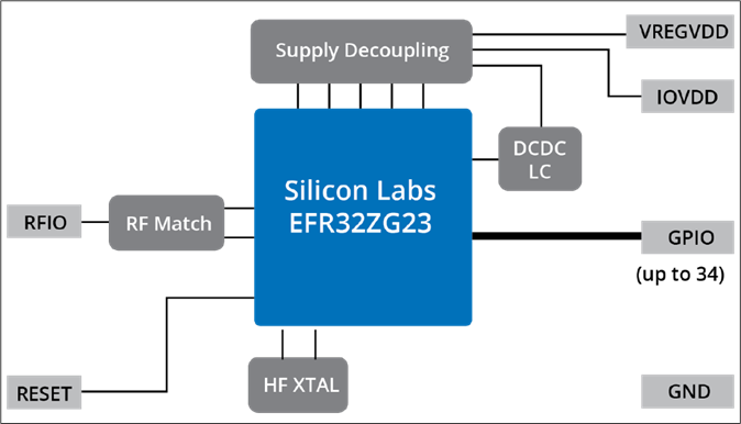
Power Supply Pins
Obviously the power supply pins are fixed function pins. The only really configurable parts to this set of pins is the voltage to apply to the IOVDD, AVDD and whether to use the on-chip DC to DC converter or not. If your device is battery powered, AVDD should be the battery voltage assuming the battery is nominally 3V (coin cells or CR123A). AVDD can be measured by the IADC in a divide by 4 mode to give an accurate voltage reading of the battery. This avoids using GPIOs and resistor dividers to measure the battery level thereby freeing up GPIOs and reducing battery drain. IOVDD should be set to whatever voltage needed by other chips on the board. Typically either 1.8 or 3.3V. The DCDC should be used in most battery powered applications unless a larger DCDC is present on the board already to power other chips.
The other configurable voltage is the RFVDD and PAVDD and the choice there depends on the radio Transmit Power you wish to use. For +14dBm PA an RF VDD are typically 1.8V. For +20dBm PAVDD must be 3.3V.
Every product has unique requirements and sources of power so I can’t enumerate all possible combinations here but follow the recommendations in the datasheets carefully. Copy the radio board or Thunderboard example schematics for most typical applications.
Debug, PTI and Trace Pins
The two Serial Wire Debug (SWD) pins (SWCLK and SWDIO) are necessary to program the chip FLASH and are the minimum required to be able to debug firmware. While it is possible to use these pins for other simple purposes like LEDs, it is best if they are used exclusively for programming/debug. These should be connected to a MiniSimplicity or other debug header.
The SWO debug pin is the next most valuable pin which can be used for debug printfs in the firmware and output to a debugging terminal. Alternatively, the UART TX and RX pins can also be used for debugging with both simple printfs and able to control the firmware using the receive side of the UART to send commands.
The two Packet Trace Interface (PTI) pins provide a “sniffer” feature for the radio. These pins are read by Simplicity Studios Network Analyzer to give a detailed view of all traffic both out of and into the radio. The main advantage of these pins is that they are exactly the received data by the radio. The Z-Wave Zniffer can also be used as a standalone sniffer thereby freeing these pins for any use. The standalone Zniffer however does not show you exactly the same traffic that the PTI pins do especially in noisy or marginal RF conditions. Thus, the PTI pins on the device provide a more accurate view of the traffic to the device under test.
The Trace pins provide additional levels of debug using the Segger J-Trace tool. These pins output compressed data that the debugger can interpret to track the exact program flow of a running program in real time. This level of debug is invaluable for debugging exceptions, interrupts, multi-tasking RTOS threads as well as tracking code coverage to ensure all firmware has been tested. Often these pins are used for other purposes that would not be necessary during firmware debug and testing. Typically LEDs or push buttons can be bypassed during trace debug. There are options to use either 4, 2 or even 1 trace data pin but each reduction in pins cuts the bandwidth and make debugging less reliable.
LFXO and EM4WU Pins
The Low Frequency Crystal Oscillator (LFXO) pins are typically connected to a 32KHz crystal to enable accurate time keeping within several seconds per day. If supporting the Time Command Class, I strongly suggest adding the 32KHz crystal. While you can rely on the LFRCO for time keeping, it can drift by as much as a minute per hour. While you can constantly get updated accurate time from the Hub every now and then, that wastes Z-Wave bandwidth and battery power. Both the Thunderboard and BRD4210 include a 32KHz crystal so you can easily compare the accuracy of each method.
Reserve the EM4WU pins for functions that need to wake the EFR32 from EM4 sleep mode. These are the ONLY pins that can wake from EM4! Note that ports PC and PD are NOT able to switch or input from peripherals while in EM2. See the datasheet and reference manual for more details.
Remaining GPIOs
Many of the remaining GPIOs have alternate functions too numerous for me to mention here. Refer to the datasheet for more details. Most GPIOs can have any of the digital functions routed to them via the PRS. Thus, I2C, SPI, UARTs, Timers and Counters can generally be connected to almost any GPIO but there are some limitations. Analog functions have some flexibility via the ABUS but certain pins are reserved for special functions. Hopefully these tables help you make wise choices about which pin to use for which function on your next Z-Wave product.


 Good news! We have added new Tech Talks. Join us on Tuesdays and Thursdays for live virtual, technical discussions hosted by a lead engineer with time allocated for your questions. We’ll cover topics like battery optimization with BG22, using Z-Wave for your Smart Home Solutions and more. You don’t want to miss these next talks.
 the router and then login to it from anywhere in the world. The system is secure and password protected. The HS3 application serves web pages with a status of every Z-Wave device. The HS3 application runs on the Raspberry Pi so all processing is local which means temporary Internet connectivity outages are no problem.