The EFR32ZG23 Z-Wave 800 series MCU has limited FLASH and RAM available for the application. The 800 series actually has less FLASH than the 700 series which stored the bootloader in a dedicated 16K memory. Worse, the bootloader in the 800 series has grown from 16K to 24K! Features are always being added to the SDK making it ever larger leaving less for the application. Seems like Silicon Labs needs to spend some time squeezing the code instead of constantly adding features.
Here is the typical error message when FLASH overflows:
Description
FLASH memory overflowed !
make: *** [makefile:114: all] Error 2
make[1]: *** [makefile:123: SwOnOff_2024120_ZG23B_GeoLoc.axf] Error 1
region `FLASH' overflowed by 92 bytes
SwOnOff_2024120_ZG23B_GeoLoc.axf section `.nvm' will not fit in region `FLASH'
We can’t create more FLASH on the chip, it has what it has. But, there’s always software we can change! By default, the project has ZAF->Z-Wave Release installed which sets the C compiler optimization to -Os which optimizes for size which is probably what we want since we’re out of FLASH. However, deep in the configuration files there is the definition for SL_BOOTLOADER_STORAGE_SIZE which changes from 196K to 180Kbytes when NDEBUG is defined. NDEBUG is defined when the Z-Wave->ZAF->Z-Wave Debug component is installed. The question of why BOOTLOADER size is being reduced by only 16K when debug is enabled is unclear to me. However, in my testing, adding the DEBUG component still results in FLASH overflowing but now by 4344 bytes! Obviously the change in Optimization from -Os to -Og (debugging) blew up the code which is expected. I enabled DEBUGPRINT to get debugging information out the UART which increased the flash usage even more.
Since I am debugging and will not be testing OTA at this stage, I don’t care how big the bootloader storage size is since I am not using it. I need more FLASH space for debugging! Simply edit the sl_storage_config.h file and change SL_BOOTLOADER_STORAGE_SIZE from 0x2C000 to 0x20000 to free up another 48K bytes:
// <o SL_BOOTLOADER_STORAGE_SIZE> Size of the bootloader storage.
// <i> Default: 0x20000
// <i> Note that this value is only being used if BOOTLOADER_STORAGE_USE_DEFAULT
// <i> is set to false. This value will control how much of the flash memory
// <i> is reserved for bootloader storage.
#if defined(NDEBUG)
#define SL_BOOTLOADER_STORAGE_SIZE  0x00030000
#else /* defined(NDEBUG) */
//#define SL_BOOTLOADER_STORAGE_SIZE  0x0002C000    - original value
#define SL_BOOTLOADER_STORAGE_SIZE  0x00020000
#endif /* defined(NDEBUG) */
Now the project fits comfortably in FLASH with plenty of left over space. However, I cannot OTA it and definitely cannot ship it in this way for production. Once I’m done debugging, I’ll have to revert back to RELEASE mode and remove DEBUGPRINT. If FLASH is overflowing that will require some additional effort to squeeze back into the available space. I would first try Link-Time-Optimization (-flto) to the C compiler but that can introduce some instability and require significant amounts of testing time. Next, try looking for code you don’t need and remove it. After that, complain to Silicon Labs they need to shrink their code!
Ram usage       :    65532 /    65532 B (100.00 %)
Flash usage     :   446868 /   491520 B ( 90.92 %)
RAM usage is at 100% is OK because the HEAP is expanded to fill the available space. But there is very little left over for the application as any RAM usage is making the HEAP smaller. The HEAP is used for all sorts of things like temporary variables, buffers and FreeRTOS. I am very concerned that some of the bugs in Z-Wave products are due to heap overflows. Heap overflows are very difficult to reproduce and debug as they typically require several failures to happen at just the right time. Unfortunately these failures seem to happen with regularity in the real world.
Hope this helps you get back to debugging quickly. Leave me a comment below with your helpful hints that I can include in a future post.
Debugging a HardFault is ROUGH, but with trace debugging, it’s a joy! A big problem with debugging firmware on a System-on-Chip (SoC) design is that the CPU and memory are encased in a plastic package severely limiting the visibility of what the CPU is doing. There are tons of interrupts and exceptions and just plain old bugs in your software that can send the CPU off into la-la land and you have no way of tracking down how it got there. Good ‘ol PRINTFs do not help since the CPU has gone off the rails. The most common method of debugging this kind of fault is to keep removing code or disabling interrupts until you magically divine the cause by inspection after a lot of tedious narrowing of possible causes and reverting checkins. In this post I’ll describe the joys of debugging using the Segger J-Trace and the Ozone debugger.
ARM CoreSight Architecture
ARM CPUs are intended to be implemented in SoCs so naturally ARM designed in a set of tools to enable visibility and debugging called the CoreSight architecture. For the embedded Cortex processors, and specifically the CM33 in the EFR32ZG23, the key components are the ARM ETMv4 which then feeds the TPIU. The ETM/TPIU tracks the CPU Program Counter (PC), packetizes changes in the PC and thus the program flow, compresses the data, then sends it out the trace pins to an external Trace Port Analyzer such as the Segger J-Trace. The Segger tools decompress and decode the trace data to match it with the image file of the compiled code to show exactly the path the program followed. ARM has a huge amount of documentation on their web site but the problem is there is too much information. ARM has many CPUs, architectures, versions and the entire ETM is an optional component with many configurable parts. This makes reading the ARM documentation much like reading the dictionary, lots of detailed information but it is tough to follow the story of how the pieces work together. Fortunately, Segger has read the documentation and figured out how to make it work.
ARM CoreSight provides CPU visibility using only 2, 3 or 5 pins
Segger J-Trace and Ozone Debugger
Segger is well known in the embedded industry for their J-Link hardware programmers, the Ozone debugger and lots of other services. They have wide support for virtually every MCU made including all of the Silicon Labs EFR32 chips. Their support for Trace debugging is excellent with reliable hardware and software. The Ozone debugger is able to read in your .AXF file out of Simplicity Studio, find all the source code, connect to the DUT via the J-Trace (which includes a J-Link for programming/debug), download the firmware in seconds and run to Main and then display the path your firmware took to get there. Easy and fast!
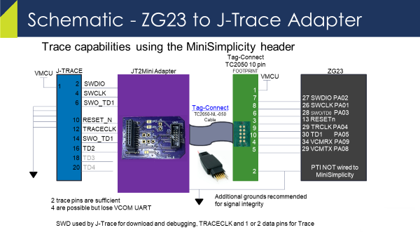
The SeggerJ-Trace Pro Cortex-M is required for Trace Debugging. While not, cheap, it’s also not expensive compared to the cost of an engineer working for days trying to capture how their firmware dropped into the weeds. The J-Trace connects to your PCB via a 20 pin header that is 50mil on centers so it is quite small. However, I’ve come up with a small PCB that lets you use the standard 10 pin MiniSimplicity header for Trace.
etm_zwave Github Repo and J2Mini Adapter
Most Z-Wave IoT products have very small PCBs and no room for another 20 pin header even if it is 50mil. I came up with a simple way to use the existing 10 pin tag-connect/MiniSimplicity header for Trace and placed all the files in a public github called etm_zwave. You do have to connect a couple of extra pins from the ZG23 to the tag-connect/MiniSimplicity header. Replace the PTI pins with the trace clock and a second data pin – the first data pin is the SWO pin already on the header. This header is tiny and you need a way to program the ZG23 anway and this is the way to go. The PTI pins are not that useful as they are only used for radio packet tracing which Z-Wave uses standalone Zniffers instead of wiring multiple nodes to the Network Analyzer. For less than $30 you can build your own JT2Mini adapter boards and then be able to use trace with just the MiniSimplicity header. You will need a extra ground connection as there is a single ground pin on the MiniSimplicity header. I’ll discuss that issue more in the troubleshooting section below.
JT2Mini adapter board plugs directly into the Segger J-Trace and MiniSimplicity cable. It only provides two trace data pins which Segger claims will only occasionally cause the CPU to stall. With 4 pins the CPU will almost never stall. Obviously with only 1 data pin you’ve cut the data rate to get the trace info out of the chip and it will stall (insert wait states) anytime the TPIU fifos will up until they are able to unload the data off-chip.
Setup Trace in Ozone
Now that the hardware is wired up, we have to enable Trace in Ozone.
Open Ozone
Include the *.JlinkScript file in the etm_zwave github repo
For the ZG23 use ZG23_Traceconfig.JLinkScript
There are comments in the file and more info in the repo ReadMe.md on how to properly insert the script into your Ozone *.jdebug project file.
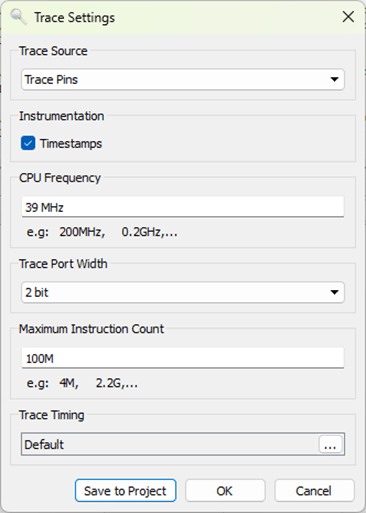
Click on Tools->Trace Settings
Change the Trace Source to Trace Pins
CPU Frequency=39MHz
Trace Port Width=2 (if using JT2Mini)
Click on Green Power button
Ozone will download the code and run to MAIN()
Open the Timeline and Code Profile windows
The TimeLine should look something like this – maybe “run” for just a fraction of a second:
This window shows how long the CPU has been in each function and the complete program flow in real time. Interrupts and switching RToS tasks are shown and make it much easier to immediately find where the hardfault occurred. Clicking in the timeline brings up the exact line of C code and optionally disassembly at that instant in time. You can quickly follow exactly where your code went wrong and the hardfault occurred.
The Timeline window also allows you to immediately see how long each function is taking. What is most important here is checking your interrupt service routines to ensure they are not busy burning a lot of CPU time doing less important work and starving other time sensitive functions. The obvious waster of time is the memset and memcpy functions which I am working on another post about those specific functions so stay tuned!
Ozone has a Code Coverage window which displays the number of lines of code that have been executed and the number of assembly instructions executed. Using this feature with a product validation suite you can quickly identify untested and potentially dead code.
Segger has plenty of training videos that go into a great deal of detail on how to use these tools. But first you need a J-Trace and get it wired up to your board.
How to get printfs via J-Trace
Unfortunately the Segger J-Trace Pro does not support the VCOM serial interface. Thus, if you want to open a terminal window and see the printfs in your code, you have to jumper the Rx/Tx pins (and ground) to a Serial to USB adapter. Fortunately I put a header on the JT2Mini PCB for exactly this purpose. The J5 header has the Rx (Pin 1 square pad) and Tx pins on it (Pin 2 round pad). J3 has ground on both pins. Use an FTDI serial to USB adapter and PuTTY or other serial terminal program to view the printfs. The DevKit EXP pins should be able to read in the serial data but I was not able to find the right combination of In/Out/MCU and AEM/Bat/USB and get SSv5 to work. Thus I recommend using a simple FTDI interface to watch the printfs when tracing.
Troubleshooting
The number one challenge with getting Trace to work is the signal integrity of the clock and the trace data pins. Once you have a clean connection, it seems to be rock stable and produces really valuable debugging data even with just two data pins. If Ozone if giving strange errors and specifically different errors with each run, odds are you have a signal integrity problem.
Yellow is Trace Data1, Green is TRACECLK – GPIOs are at max bandwidth
The EFR32 Series 2 (including the ZG23) GPIOs have only a 20MHz bandwidth. The Trace clock is a divide by 2 of the 39MHz CPU clock so it is running right at the maximum of the GPIO. Trace data is clocked out on both edges of the clock. Since the MiniSimplicity header has only 1 ground on it and there are at least 3 GPIOs toggling at their maximum rates, the signal integrity is marginal even in the best of circumstances. The JT2Mini has extra ground pins and I highly recommend connecting them with additional jumper wire while using Trace. The cable from your board to the JT2Mini should also be no more than 6 inches long. The .JlinkScript file has code in it for adjusting the slew rate of the GPIOs which can improve or possibly degrade the trace signal integrity. Ozone and J-Trace can also adjust the relative timing of the CLK to the data with sub-nanosecond resolution. You’ll have to experiment on your own if you are having problems.
Conclusion
I can’t live without Trace debugging. I don’t necessarily use it all the time but I will wire it up to every board I design in the future! I have spent weeks debugging hardfaults in the past and then solve the problem in 10 minutes using Trace. Get one for yourself!
See many of you next week at the Z-Wave Summit in Orlando Florida where I will be giving a presentation on The Joys of Trace Debugging and running the UnPlugFest on Monday!
Z-Wave Long Range (ZWLR) claims to reach over 1 mile, but does it actually reach that far in the real world? The answer is YES. However, in the real world we are operating inside a building and surrounded by trees and other buildings. The more important answer is how does ZWLR do in a building and in an neighborhood? I recently captured some data in my home town just outside of Boston which shows ZWLR easily reaches the entire yard and then some.
The first thing to understand about the RF range of Z-Wave are the different power levels used by regular Z-Wave (ZW) and ZWLR. I’m comparing the values used in the US but the rules are different in each region. In the EU the max transmit power is +13dBm with regular Z-Wave which is why the range in the EU is so much further than in the US. But let’s focus just on the US for now.
RF Transmit Power
There are 3 levels of Z-Wave RF transmit power in the US:
-1dBm – Regular Z-Wave GFSK modulation – 12mA
+14dBm – ZWLR DSSS-OQPSK modulation – 41mA
+20dBm – ZWLR DSSS-OQPSK modulation – 92mA
The huge increase in transmit power is why ZWLR has over double the range of ZW. The reason ZWLR can transmit at such high power levels is that the spread spectrum modulation spreads that energy across a 1MHz carrier compared to the narrow band FSK of ZW. The FCC allows the transmit power to be as high as +30dBm but that would be a challenge for a battery powered device as it would likely need half an amp of current!
Why are there two power levels for ZWLR? The RF transmit power is matched to the power supply of the typical use case. The ZGM230 module is limited to +14dBm since it is most often used in battery powered devices where even the 41mA current is a bit challenging for low-cost batteries. The +20dBm ZG23 is best suited to mains-powered devices to get the maximum range. ZWLR utilizes dynamic RF power so for nodes that are close enough, the battery life is extended by using only enough RF power to reliably reach the controller. the dynamic power algorithm is built into the Z-Wave protocol so you don’t have to manage it at all.
RF Range at Home
The Yellow circle is the regular Z-Wave mesh range with a controller in a room on the 2nd floor. My home is surrounded by large pine trees which limit the range. Using 700/800 series Z-Wave chips there are no dead spots anywhere in my home. I still have a few 100 series devices, several 300 series and a lot of 500 series devices many of which need the mesh to hop to reach my controller. This demonstrates the increasing range of each generation of Z-Wave. If I were to upgrade all of my devices there would be little if any routing using regular ZW.
The Red circle shows over double the range of regular Z-Wave at +14dBm. The combination of higher transmit power and increased sensitivity due to the spread spectrum modulation yields a strong signal over my entire neighborhood. Note the bump on the right side caused by the open field and the swampy area with a lot fewer trees. Each wall or tree or building reduces the range but ZWLR easily reaches well beyond the end of the yard. I couldn’t test 20dBm because there just isn’t enough open space for me to measure it! So I moved to a building in the center of town.
RF Range in Town
The photo above shows the relative range of all three transmit powers. In this case the controller is in the upper right corner of a commercial building as shown in the inset in the lower left. Regular Z-Wave is not quite able to reach the two rooms at the far end of this 35m building. But ZWLR easily reaches the entire building and well beyond. Each step, +14 and then +20 roughly doubles the range in this typical application where there are still a number of trees and buildings reducing the signal. Recall from middle school geometry that the circumference of a circle is 2*pi*radius or roughly 6*radius. On the day I performed this test, I doubled my daily step goal and walked over 20,000 steps!
In both of these measurements the line is roughly where full 2-way, fully secure, supervision encapsulated Basic Set commands were being sent to a battery powered SwitchOnOff sample application using SDK 7.18.3. I used a Raspberry Pi running Unify and a small python program to send Basic Set On/Off commands every half second to the Dev Kit and then noted where the LED stopped blinking. Once I stepped a few paces back toward the controller, the two devices would resync and the blinking would restart. Z-Wave is very adept at re-connecting to devices that are at the margin of the RF range.
During the Z-Wave summit earlier this month we did a live demonstration of the range versus the transmit power. While regular Z-Wave reached well beyond the conference center, it couldn’t quite get to the adjacent hotel. ZWLR however reliably reached the hallways in the hotel thru the concrete and glass of each building.
How to Set Tx Power
For regular Z-Wave the transmit power is normally set pretty close to the maximum of -1dBm. There are two configuration parameters to set based on the results of FCC testing. See INS14664 in Simplicity Studio for details. For ZWLR, setting the transmit power easier. Simply set APP_MAX_TX_POWER_LR in zw_config_rf.h to either 140 for +14dBm or 200 for +20dBm but that only works if the EFR you are using supports +20. The 700 series EFR32ZG14 supports +20 but the balun has to be wired to +3.3V to have enough power to reach +20. The ZGM130/230 are both limited to just +14. The EFR32ZG23 part number chooses either +14 or +20 – EFR32ZG23B0X0F512 – If the X is 1 it’s +14, if 2 then +20.
One last configuration setting is to make sure ZWLR is enabled. This is in zw_region_config.h and all you need to do is set it to REGION_US_LR. The protocol code completely handles everything relative to ZW or ZWLR for you so just a 3 character change enables ZWLR.
Conclusion
All new Z-Wave devices for the US market should support Z-Wave Long Range. The low-latency (no routing), high reliability and long range make it a must for any new product. The question is +14 or +20? All controllers should be using the SoC (EFR32ZG23A/B020) to get the most range. The SoC requires calibration of the crystal for each unit as described in UG517. The module (ZGM130/ZGM230) are limited to +14 only and come pre-calibrated from Silicon Labs and thus are ideal for end devices that are battery powered. The SoC should be used for any mains-powered end device since the current draw is not an issue but be careful to specify the right part number with the 020 in it.
Have you always wanted your very own Z-Wave widget-thing-a-ma-bob-doohickey? Silicon Labs recently released the Thunderboard Z-Wave (TBZ) which is an ideal platform for building your own Z-Wave device. Officially known as the ZGM230-DK2603A, the TBZ has sensors galore, expansion headers to connect even more stuff, comes with a built-in debugger via USB-C and can be powered with a single coin cell. Totally cool! I am working on a github repo for the TBZ but right now there are three simple sample apps in Simplicity Studio to get started.
ZGM230 Z-Wave Long Range Module – +14dBm radio – 1mi LOS RF range
ARM Cortex-M33, 512/64K FLASH/RAM, UARTs, I2C, SPI, Timers, DAC/ADC and more
Built-in Segger J-Link debugger
USB-C connectivity for SerialAPI and/or debugging
RGB LED, 2 yellow LEDs, 2 pushbuttons
Temperature/Humidity sensor
Hall Effect sensor
Ambient Light sensor
6-Axis Inertial sensor
Metal sensor
1Mbyte SPI FLASH
Qwiic I2C connector
Break-out holes
SMA connector for antenna
Coin cell, USB or external power
Firmware development support via Simplicity Studio
Sample Applications
There are three sample applications in Simplicity Studio at the time of this writing (Aug 2022 – SDK 7.18.1);
SerialAPI,
SwitchOnOff
SensorMultilevel
The TBZ ships with the SerialAPI pre-programmed into it so you can use it as a Z-Wave controller right out of the box. Connect the TBZ to a Raspberry Pi or other computer to build a Z-Wave network. Use the Unify SDK to get a host controller up and running quickly or use the PC-Controller tool within Simplicity Studio for development and testing. The SwitchOnOff sample app as the name implies simply turns an LED on/off on the board via Z-Wave. This is the best application to get started as the ZGM230 chip is always awake and is easy to debug and try out. The SensorMultilevel sounds like a great app as it returns a temperature and humidity but at the moment it does not use the sensor on the TBZ and simply always returns a fixed value. SensorMultilevel shows how to develop a coin-cell powered device. Additional sample apps are expected to be available in future SDK releases but I am working on a github repo with a lot of sensor support.
Naturally a single Z-Wave Node doesn’t do much without a network. You’ll need some sort of a hub to connect to. Most of the common hubs (SmartThings, Hubitat, Home Assistant, etc) will at least let you join your widget to the network and do some basic control or status reporting. You need either a pair of TBZs or perhaps purchase the even cheaper UZB7 for the controller side and then the TBZ for the end-device. Then you have a network and can build your doohickey and talk to it over the Z-Wave radio.
Getting Started
Plug in the TBZ to your computer and open Simplicity Studio which will give you a list of applicable documents including the TBZ User Guide. Writing code for the TBZ definitely requires strong C programming skills. This is not a kit for an average Z-Wave user without strong programming skills. There is a steep learning curve to learn how to use the Z-Wave Application Firmware (ZAF) so only experienced programmers should take this on. I would recommend watching the Unboxing the 800 series video on the silabs web site to get started using Simplicity Studio. I hope to make a new video on the TBZ and publish the github repo so stay tuned.
Have you created a Thing-a-ma-bob using the TBZ? Let me know in the comments below!
The two Z-Wave 800 series chips from Silicon Labs have flexible GPIOs but figuring out which one is the best for which function can be challenging. There are a number of restrictions based on the function and the energy (sleep) mode you need the GPIO to operate in. Similar to my posting on the 700 series, this post will guide you to make wise decisions on which pin to use for which function.
The tables below are a compilation of several reference documents but all of the data here was manually copied out of the documents and I could have made a mistake or two. Please post a comment if you see something wrong and I’ll fix it right away.
The table below lists the pins from the most flexible to the most fixed function. There are more alternate functions than the ones listed in this table. The most commonly used alternate functions are listed here to keep the table readable. Refer to the schematics and datasheets for more details.
Port A and B are operational down to EM2, other GPIOs will retain their state but will not switch or pass inputs. Thus, use port A and B for anything special and use C and D for simple things not needed when sleeping (LEDs, enables, etc).
WSTK GPIO Probe Points
Only the ZG23 QFN48 pin numbers are listed in the table. The QFN48 is expected to be pin compatible with future version of the ZG23 with additional Flash/RAM so I recommend using it over the QFN40. The WSTK2 is the Pro DevKit board with the LCD on it which comes as part of the PK800 kit. There are two sets of holes labeled with Pxx numbers on them which are handy to probe with an oscilloscope. The Thunderboard Z-Wave (TBZ) also has 2 rows of holes which are ideal for probing or connecting to external devices for rapid prototyping.
Name
ZG23
ZGM230
WSTK2
TBZ
ALT FUNC
Comments
PB2
22
9
P19
EXP5 BTN1
Use the pins at the top of this list first as they are the most flexible
PB6
NA
5
EXP15 I2CSDA
TBZ Qwiic I2C_SDA
PB5
NA
6
EXP16 I2CSCL
TBZ Qwiic I2C_SCL
PB4
NA
7
PA10
35
23
PC1
2
35
P1
EXP4
PC and PD are static in EM2/3
PC2
3
36
P3
EXP6
PC3
4
37
P5
EXP8
PC4
5
38
P35
BLUE
PC6
7
40
P33
EXP9
PC8
9
42
P31
LED0
PC9
10
43
P37
LED1
PD3
45
30
P26
IMUEN
PB0
24
11
P15
VDAC0CH0
PA0
25
12
P2
GREEN
IDACVREF
PB1
23
10
P17
RED
EM4WU3 VDAC0CH1
EM4WUx pins can wake up from EM4 sleep mode on a transition of the GPIO
PB3
21
8
P21
EXP3 BTN0
EM4WU4
PC0
1
34
P7
EXP10
EM4WU6
PC5
6
39
P12
EXP7
EM4WU7
PC7
8
41
P13
SNSEN
EM4WU8
PD2
46
31
P6
EXP11
EM4WU9
PD0_LFXTAL_O
48
33
XC32
XC32
BRD4210 and TBZ have 32KHz crystal mounted
PD1_LFXTAL_I
47
32
XC32
XC32
Accurate timing while sleeping – Time CC
PA7
32
20
P10
TraceD3
Trace pins for debug & code coverage
PA6
31
19
P8
TraceD2
Trace is configurable for 4, 2 or 1 data pin
PA5
30
17
P4
IMUINT
EM4WU0 TraceD1
PA4_TDI
29
16
P41
EXP13
JTAG_TDI TraceCLK
JTAG data in Trace Clock out
Pins below here should be used primarily for debug
PD4_PTIDATA
44
29
P25
Packet Trace Interface (PTI) data
PD5_PTISYNC
43
28
P24
EM4WU10
PTI Sync
PA9_URX
34
22
P11
EXP14
VCOM UART
PA8_UTX
33
21
P9
EXP12
VCOM UART
PA3_SWO
28
15
P16
JTAG_TDO TraceD0
RTT UART printf and Trace D0
PA2_SWDIO
27
14
P18
JTAG_TMS
These two SWD pins should ONLY be used for debug and programming
PA1_SWCLK
26
13
P20
JTAG_TCK
SWD debug clock
Pins below here are fixed function only
SUBG_O1
18
NA
Not used by Z-Wave
SUBG_I1
16
NA
Not used by Z-Wave
SUBG_O0
19
3
RFIO on ZGM230
SUBG_I0
17
NA
Matching network to SMA
RESET_N
13
1
F4
Push buttons on DevKit boards
HFXTAL_O
12
NA
39MHz crystal
HFXTAL_I
11
NA
39MHz crystal
DECOUPLE
36
18
1.0uF X8L cap (unconnected on ZGM230)
VREGSW
37
NA
Inductor to DVDD for DCDC – 3.3V
VREGVDD
38
25
3.3V In/Out based on mode
DVDD
40
24
VDCDC on ZGM230
AVDD
41
NA
Highest voltage – typically battery voltage
IOVDD
42
26
1.8-3.8V
PAVDD
20
NA
3.3V for +20, 1.8V for +14dBm
RFVDD
14
NA
1.8V or 3.3V but less than PAVDD
VREGVSS
39
27, 44
GND
RFVSS
15
2, 4
GND
Power Supply Pins
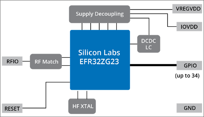
Obviously the power supply pins are fixed function pins. The only really configurable parts to this set of pins is the voltage to apply to the IOVDD, AVDD and whether to use the on-chip DC to DC converter or not. If your device is battery powered, AVDD should be the battery voltage assuming the battery is nominally 3V (coin cells or CR123A). AVDD can be measured by the IADC in a divide by 4 mode to give an accurate voltage reading of the battery. This avoids using GPIOs and resistor dividers to measure the battery level thereby freeing up GPIOs and reducing battery drain. IOVDD should be set to whatever voltage needed by other chips on the board. Typically either 1.8 or 3.3V. The DCDC should be used in most battery powered applications unless a larger DCDC is present on the board already to power other chips.
The other configurable voltage is the RFVDD and PAVDD and the choice there depends on the radio Transmit Power you wish to use. For +14dBm PA an RF VDD are typically 1.8V. For +20dBm PAVDD must be 3.3V.
Every product has unique requirements and sources of power so I can’t enumerate all possible combinations here but follow the recommendations in the datasheets carefully. Copy the radio board or Thunderboard example schematics for most typical applications.
Debug, PTI and Trace Pins
The two Serial Wire Debug (SWD) pins (SWCLK and SWDIO) are necessary to program the chip FLASH and are the minimum required to be able to debug firmware. While it is possible to use these pins for other simple purposes like LEDs, it is best if they are used exclusively for programming/debug. These should be connected to a MiniSimplicity or other debug header.
The SWO debug pin is the next most valuable pin which can be used for debug printfs in the firmware and output to a debugging terminal. Alternatively, the UART TX and RX pins can also be used for debugging with both simple printfs and able to control the firmware using the receive side of the UART to send commands.
The two Packet Trace Interface (PTI) pins provide a “sniffer” feature for the radio. These pins are read by Simplicity Studios Network Analyzer to give a detailed view of all traffic both out of and into the radio. The main advantage of these pins is that they are exactly the received data by the radio. The Z-Wave Zniffer can also be used as a standalone sniffer thereby freeing these pins for any use. The standalone Zniffer however does not show you exactly the same traffic that the PTI pins do especially in noisy or marginal RF conditions. Thus, the PTI pins on the device provide a more accurate view of the traffic to the device under test.
The Trace pins provide additional levels of debug using the Segger J-Trace tool. These pins output compressed data that the debugger can interpret to track the exact program flow of a running program in real time. This level of debug is invaluable for debugging exceptions, interrupts, multi-tasking RTOS threads as well as tracking code coverage to ensure all firmware has been tested. Often these pins are used for other purposes that would not be necessary during firmware debug and testing. Typically LEDs or push buttons can be bypassed during trace debug. There are options to use either 4, 2 or even 1 trace data pin but each reduction in pins cuts the bandwidth and make debugging less reliable.
LFXO and EM4WU Pins
The Low Frequency Crystal Oscillator (LFXO) pins are typically connected to a 32KHz crystal to enable accurate time keeping within several seconds per day. If supporting the Time Command Class, I strongly suggest adding the 32KHz crystal. While you can rely on the LFRCO for time keeping, it can drift by as much as a minute per hour. While you can constantly get updated accurate time from the Hub every now and then, that wastes Z-Wave bandwidth and battery power. Both the Thunderboard and BRD4210 include a 32KHz crystal so you can easily compare the accuracy of each method.
Reserve the EM4WU pins for functions that need to wake the EFR32 from EM4 sleep mode. These are the ONLY pins that can wake from EM4! Note that ports PC and PD are NOT able to switch or input from peripherals while in EM2. See the datasheet and reference manual for more details.
Remaining GPIOs
Many of the remaining GPIOs have alternate functions too numerous for me to mention here. Refer to the datasheet for more details. Most GPIOs can have any of the digital functions routed to them via the PRS. Thus, I2C, SPI, UARTs, Timers and Counters can generally be connected to almost any GPIO but there are some limitations. Analog functions have some flexibility via the ABUS but certain pins are reserved for special functions. Hopefully these tables help you make wise choices about which pin to use for which function on your next Z-Wave product.
Here we go again… Once again I’ve been given yet another board with randomly placed test points instead of a nice neat, reliable header to connect via my MiniSimplicity cable. So I’m spending an hour on my microscope soldering thin little wires to the tiny little test points to be able to flash and then debug the firmware on a new ZG23 based product. Once I’m done soldering, I’m left with a very fragile board which is unreliable at best and at worst will result in even less hair on my thinning head. My post from 2019 described using a zero cost header for a reliable connection, but it seems not everyone is reading my blog!
On the flip side, a different customer sent me their board with a Tag-ConnectEdge-Connect that I had not seen before but is absolutely brilliant. The Edge-Connect uses the EDGE of your PCB for the test points. Barely 1mm wide and about 20mm long it is possible to include this debug connector on virtually any PCB. There is a locking pin to hold the cable secure while the spring loaded tabs press into the castellated notches to ensure solid contact.
Close up of the locking pin and castellated notches
There are several sizes of the Edge-Connect but the recommended one is the 10-pin EC10-IDC-050 which matches the MiniSimplicity header on the WSTK DevKit board. Note that the the 6pin cable in the photo above is NOT the one I would recommend but it was the only one in stock at the time and it worked fine for debugging but doesn’t have the UART or PTI pins.
Tag-Connect has many other types of debug headers/cables of various configurations to hold the cable to the PCB securely. The original Tag-Connect cables have plastic clips that snap into fairly large thru-holes in your PCB. While this is a reliable connection, the thru-holes eat up a lot of PCB real estate. The next evolution was to use a small retaining clip under the PCB that grips onto the metal alignment pins. The photo below shows the PCB pads are not much bigger than an 0805 footprint and only requires three small thru-holes.
Note the smallest header is about the same as an 0805 in lower left corner
The lowest cost approach is to simply add a 10-pin header footprint on your PCB that matches the pinout of the MiniSimplicity header. See section 5.1.1 of Application Node AN958 for the pinout of the 10-pin MiniSimplicity header. You don’t need to solder the header onto the PCB except when debugging. Thus the header can be under a battery or some relatively inaccessible location as when you are debugging in the lab the PCB is usually not installed in the product enclosure.
Please use ANY of these standard connectors on your next project. Without a solid connection between your computer and the chip you will find yourself chasing ghosts and losing hair.
The new Z-Wave 800 Series silicon is now shipping in volume and fully supported by the Silicon Labs tools so it’s time to get to work designing new products! In this post I’ll describe the main advantages and the difference between the chip version (SoC) and the module. But first I want to invite everyone to watch the Tech Talk on using the new 800 series developers kit: ZWAVE-PK800A.
I am presenting the new Z-Wave Developers Kit – ZWAVE-PK800A in a webinar on 22 March 2022. The webinar is recorded so if you missed it, you can still view it anytime, just click the image.
Unlike the 700 series, either the SiP module or the SoC can be used for either controllers or end devices. In the 700 series the EFR32ZG14 SoC is only usable on gateways and only runs the SerialAPI. The ZGM130 module is used for all end devices and can be used on gateways. Thus, the 800 series gives you more choices for which chip/module to use that best matches your product needs.
What’s the difference between 800 series Module vs. SoC?
Here’s the short list of differences:
ZGM230S SiP Module – easier to use
Integrated crystal, RF match, decoupling
Factory calibrated CTUNE
34 GPIO – 44 pin SiP 6.5×6.5mm
+14dBm Max RF Transmit power (lower battery current targeting End Devices)
More expensive unit cost but just add antenna and a few passives
23/31 GPIO – 40/48 QFN 5×5/6x6mm (48 pin compatible with a future larger flash/ram device)
+14dBm or +20dBm Z-Wave Long Range RF Tx power
Line powered devices should use +20 for additional RF Range
Lower unit cost but more companion parts, antenna and crystal calibration required
Both require an external antenna and require regulatory (FCC/CE) testing
ZGM230S Module
The ZGM230S System-in-Package (SiP) Module is a superset of the EFR32ZG23 System-on-Chip (SoC). The module adds a handful of inductors and capacitors for the DC-to-DC regulator and RF matching and the 39MHz crystal which is pre-calibrated at the Silicon Labs factory. The module is easier to manufacture (fewer components and no calibration) but is limited to +14dBm transmit power in Z-Wave Long Range. Modules are more expensive due to the integration but the cost crossover is at pretty high volumes.
ZGM230S SiP Module contains the ZG23 SoC chip, a calibrated crystal and a few passive components
ZG23 SoC
The ZG23 SoC is the chip inside the module. The main advantage of using the SoC is that at high volumes, it is cheaper. The SoC supports +20dBm Z-Wave Long Range transmit power which can nearly double the radio range over the module. But +20dBm demands a lot of battery power so it typically cannot be powered with coin cells but must use a CR123A or AA batteries. Getting FCC to pass at +20dBm can also be a challenge and careful matching of the antenna is required. On the factory test floor, every unit manufactured must have the 39MHz crystal calibrated. Details of the calibration process are described in User Guide 522. The crystal calibration is necessary to ensure reliable radio communication and is a process that requires a spectrum analyzer and several seconds of testing. Your manufacturing partner has to be equipped and knowledgeable to properly calibrate each unit efficiently.
500 vs. 700 vs. 800 Series Comparison
Are you still working with the Z-Wave 500 series and need more details on which series to upgrade to? Fortunately we’ve put together this comparison table to answer those questions. I have to say that once you’ve written and debugged code for a modern ARM processor, you will NEVER want to use the 500 series 8051 8-bit CPU ever again!
Which Z-Wave Series to use?
In these times of long lead times and limited silicon availability, the main question of which Z-Wave chip/module to use may come down to which ones you can get! Silicon Labs keeps some inventory of all of our chips available thru our distributors Digikey, Mouser and Arrow. Each day a few hundred chips of all types are placed into inventory so anyone can buy enough to build prototypes. If there are zero available today, try again tomorrow or the next day. At this time (end of Q1 2022), we are able to supply the 500 series pretty well but the supply outlook for 2023 is uncertain. The 700 series has limited availability so if you already have orders placed and have been given allocation, you are OK. The 800 series is our most advanced process which Silicon Labs and our fabrication partners are investing in upgrading capacity so availability will improve late in 2022 and into 2023. Any new product development or upgrading of 500 series products should use the 800 series. This outlook changesliterally daily so contact your Silicon Labs sales person for the latest recommendation.
Conclusion
The choice of 800 series is easy – do it! The improvements and availability over the 500 and 700 series makes using the 800 series a no-brainer. So the next question is Module or SoC? That decision has to be done on a case-by-case basis as there are a lot of factors to be weighed. The first hurdle is the total unit volume you expect to purchase. If you’re not in the 100,000+ per year stage, then the recommendation is to use the module as it is simply easier to manufacture. The crystal calibration requirement for the SoC is non-trivial and demands expertise and equipment to do it properly. If your target market is not the US, then the module is also the way to go as the additional RF power isn’t available except in the US region as Z-Wave Long Range is only available in North America. I recommend you contact your local FAE to discuss your needs and we’ll help guide to the appropriate solution that balances cost vs. complexity.