To use an RTOS for your embedded project, or Not! That is the question poor Yorick! I digress from my usual focus on Z-Wave to discuss the general topic of using a Real-Time Operation System (RTOS) for simple embedded IoT devices. The question is moot for Z-Wave since the protocol has FreeRTOS built-in starting with the release of the 700 series. For the moment at least, the choice is To RTOS!
What is an RTOS?
My focus in this post is on small IoT devices like sensors, dimmers, window shades, to more complex devices like thermostats and door locks. Using an RTOS for simple devices like these brings different requirements than say a full Operating System like Windows or Linux. The purpose of an Operating System (OS) is to provide common resources to an application – things like memory management and insulating the application from hardware . The term “Real-Time” comes from basic concept of dividing up the resources of an embedded system so that tasks are completed within a certain timeframe. A hard-real-time system is often used in demanding applications like Engine Control. The precise management of firing the spark plugs at exactly the proper microsecond is critical to the efficient operation of an internal combustion engine. But simple IoT devices have much lower demands on the RTOS and instead are attracted to the coding efficiency and standardization of an RTOS – this is often called a soft-RTOS. All this comes at a cost in CPU and memory resources so the question remains – is an RTOS worth it for simple IoT devices?
FreeRTOS Features:
Trusted Reliable Kernel
MultiTasking/MultiThreaded
Mailboxes, Mutexes, Queues
Modular Libraries
Broad Eco-System support – 40+ MCU architectures
Small Scalable kernel size with power saving modes
Complete online documentation
Long Term Stable Support – Active support Community
Completely Free Open Source project
Z-Wave History with FreeRTOS
In the beginning Z-Wave ran on an 8-bit MCU with limited FLASH and RAM which meant life without an RTOS due to CPU performance and memory limitations. The Z-Wave protocol was built on “Bare Metal” and thus interrupt driven with a tick-timer and drivers to provide basic services. The 700 series opened the world of a 32-bit RISC MCU and significantly more memory which enabled the use of an RTOS as the foundation of the Z-Wave protocol.
I was a Field Applications Engineer for Silicon Labs for several years and in that time I would guess easily half the bugs I came across were caused by the complexity of the RTOS. I don’t have any hard statistics but it certainly seemed that way to me! The Z-Wave protocol code was ported from a Bare-Metal implementation on an 8-bit CPU to a 32-bit ARM running FreeRTOS – a challenging port to say the least! The developers treated FreeRTOS like a black-box (which is the whole point of an RTOS) and often made small mistakes that turned into really difficult to debug problems. Things like: not checking when a queue is full, not using the *FromISR() version of various calls inside interrupt service routines, hidden stack overflows by not enabling overflow checking, incomplete configuration of the many, many, many options just to name a few. An RTOS adds a LOT of complexity but you get a lot of features. The developers have to be fully trained and understand the best practices for using the complexity of the RTOS to achieve a robust system.
My primary complaint with the current implementation is that it continues to be pre-compiled into the Z-Wave library. More and more of the configuration files and various parts of FreeRTOS have been moved out of the library and into source code with each SDK release. Moving the entire RTOS into source form is not exposing any proprietary code – after all, it’s open source! It would allow developers to more quickly move to newer releases of the RTOS and related libraries. Perhaps this will come as part of the Open Source Work Group (OSWG) in the Z-Wave Alliance. We’ll have to wait and see…
The Case FOR an RTOS – Pros
I want to again note that I am talking about using an RTOS for small IoT devices. There are many other applications and environments for an RTOS which have different Pros/Cons. A few of the main features of an RTOS for IoT are:
Measuring the complexity and bug rate introduced by an RTOS unfortunately can’t be quantitatively measured. I contend that in the case of Z-Wave the complexity has outweighed the benefits. The “features” of an RTOS lead to its complexity. For one task to communicate with another, you need to setup queues in both directions. That’s a lot of code and RAM where a simple handshake would most likely do the job as was done in the Bare Metal days.
Complexity
Resource Usage – CPU, FLASH, RAM
Development Tools
Training of developers
Final Thoughts
Simple devices like light switches, sensors, window shades, and the like barely need an RTOS. These simple devices rarely need multiple tasks or the other features compared to the complexity added. More complex devices like thermostats and door locks often have a high performance application CPU where even more resources are available for things like OLED screen drivers and fingerprint readers. In this case, the Z-Wave chip is relegated to a minor role of just providing wireless connectivity which again does not need an RTOS. All that being said, the current Z-Wave protocol is fundamentally based on FreeRTOS so the To RTOS or Not To RTOS question has already been settled – To RTOS we go!
One final point on code reuse – I find Code Reuse to be a double edge sword. One the one hand, the name sounds very attractive – code once, use many times. The reality is that most code is not reusable and in the effort to make it modular, more bugs are introduced than are saved. In many cases I can write a function in a fraction of the lines of code compared to the “driver” that does it all for every flavor of chip. There’s many research papers that discuss that bugs/line of code is fairly constant. So the fewer lines of code, the fewer bugs. The fewer lines of code the easier to read and to test. Not to say that all reusable code is bad and certainly code that has been extensively tested in many ways is super valuable, but every engineer needs to make that judgement for their specific application. That’s why you get paid the big bucks!
Have you always wanted your very own Z-Wave widget-thing-a-ma-bob-doohickey? Silicon Labs recently released the Thunderboard Z-Wave (TBZ) which is an ideal platform for building your own Z-Wave device. Officially known as the ZGM230-DK2603A, the TBZ has sensors galore, expansion headers to connect even more stuff, comes with a built-in debugger via USB-C and can be powered with a single coin cell. Totally cool! I am working on a github repo for the TBZ but right now there are three simple sample apps in Simplicity Studio to get started.
ZGM230 Z-Wave Long Range Module – +14dBm radio – 1mi LOS RF range
ARM Cortex-M33, 512/64K FLASH/RAM, UARTs, I2C, SPI, Timers, DAC/ADC and more
Built-in Segger J-Link debugger
USB-C connectivity for SerialAPI and/or debugging
RGB LED, 2 yellow LEDs, 2 pushbuttons
Temperature/Humidity sensor
Hall Effect sensor
Ambient Light sensor
6-Axis Inertial sensor
Metal sensor
1Mbyte SPI FLASH
Qwiic I2C connector
Break-out holes
SMA connector for antenna
Coin cell, USB or external power
Firmware development support via Simplicity Studio
Sample Applications
There are three sample applications in Simplicity Studio at the time of this writing (Aug 2022 – SDK 7.18.1);
SerialAPI,
SwitchOnOff
SensorMultilevel
The TBZ ships with the SerialAPI pre-programmed into it so you can use it as a Z-Wave controller right out of the box. Connect the TBZ to a Raspberry Pi or other computer to build a Z-Wave network. Use the Unify SDK to get a host controller up and running quickly or use the PC-Controller tool within Simplicity Studio for development and testing. The SwitchOnOff sample app as the name implies simply turns an LED on/off on the board via Z-Wave. This is the best application to get started as the ZGM230 chip is always awake and is easy to debug and try out. The SensorMultilevel sounds like a great app as it returns a temperature and humidity but at the moment it does not use the sensor on the TBZ and simply always returns a fixed value. SensorMultilevel shows how to develop a coin-cell powered device. Additional sample apps are expected to be available in future SDK releases but I am working on a github repo with a lot of sensor support.
Naturally a single Z-Wave Node doesn’t do much without a network. You’ll need some sort of a hub to connect to. Most of the common hubs (SmartThings, Hubitat, Home Assistant, etc) will at least let you join your widget to the network and do some basic control or status reporting. You need either a pair of TBZs or perhaps purchase the even cheaper UZB7 for the controller side and then the TBZ for the end-device. Then you have a network and can build your doohickey and talk to it over the Z-Wave radio.
Getting Started
Plug in the TBZ to your computer and open Simplicity Studio which will give you a list of applicable documents including the TBZ User Guide. Writing code for the TBZ definitely requires strong C programming skills. This is not a kit for an average Z-Wave user without strong programming skills. There is a steep learning curve to learn how to use the Z-Wave Application Firmware (ZAF) so only experienced programmers should take this on. I would recommend watching the Unboxing the 800 series video on the silabs web site to get started using Simplicity Studio. I hope to make a new video on the TBZ and publish the github repo so stay tuned.
Have you created a Thing-a-ma-bob using the TBZ? Let me know in the comments below!
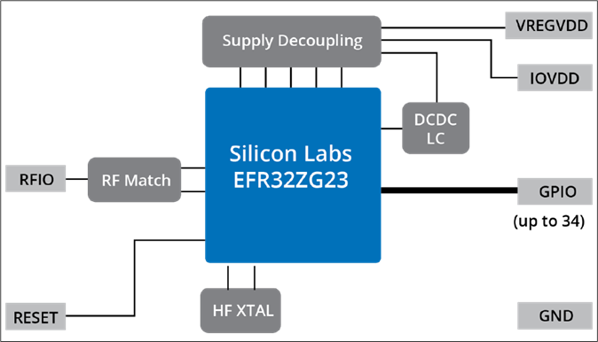
The two Z-Wave 800 series chips from Silicon Labs have flexible GPIOs but figuring out which one is the best for which function can be challenging. There are a number of restrictions based on the function and the energy (sleep) mode you need the GPIO to operate in. Similar to my posting on the 700 series, this post will guide you to make wise decisions on which pin to use for which function.
The tables below are a compilation of several reference documents but all of the data here was manually copied out of the documents and I could have made a mistake or two. Please post a comment if you see something wrong and I’ll fix it right away.
The table below lists the pins from the most flexible to the most fixed function. There are more alternate functions than the ones listed in this table. The most commonly used alternate functions are listed here to keep the table readable. Refer to the schematics and datasheets for more details.
Port A and B are operational down to EM2, other GPIOs will retain their state but will not switch or pass inputs. Thus, use port A and B for anything special and use C and D for simple things not needed when sleeping (LEDs, enables, etc).
WSTK GPIO Probe Points
Only the ZG23 QFN48 pin numbers are listed in the table. The QFN48 is expected to be pin compatible with future version of the ZG23 with additional Flash/RAM so I recommend using it over the QFN40. The WSTK2 is the Pro DevKit board with the LCD on it which comes as part of the PK800 kit. There are two sets of holes labeled with Pxx numbers on them which are handy to probe with an oscilloscope. The Thunderboard Z-Wave (TBZ) also has 2 rows of holes which are ideal for probing or connecting to external devices for rapid prototyping.
Name
ZG23
ZGM230
WSTK2
TBZ
ALT FUNC
Comments
PB2
22
9
P19
EXP5 BTN1
Use the pins at the top of this list first as they are the most flexible
PB6
NA
5
EXP15 I2CSDA
TBZ Qwiic I2C_SDA
PB5
NA
6
EXP16 I2CSCL
TBZ Qwiic I2C_SCL
PB4
NA
7
PA10
35
23
PC1
2
35
P1
EXP4
PC and PD are static in EM2/3
PC2
3
36
P3
EXP6
PC3
4
37
P5
EXP8
PC4
5
38
P35
BLUE
PC6
7
40
P33
EXP9
PC8
9
42
P31
LED0
PC9
10
43
P37
LED1
PD3
45
30
P26
IMUEN
PB0
24
11
P15
VDAC0CH0
PA0
25
12
P2
GREEN
IDACVREF
PB1
23
10
P17
RED
EM4WU3 VDAC0CH1
EM4WUx pins can wake up from EM4 sleep mode on a transition of the GPIO
PB3
21
8
P21
EXP3 BTN0
EM4WU4
PC0
1
34
P7
EXP10
EM4WU6
PC5
6
39
P12
EXP7
EM4WU7
PC7
8
41
P13
SNSEN
EM4WU8
PD2
46
31
P6
EXP11
EM4WU9
PD0_LFXTAL_O
48
33
XC32
XC32
BRD4210 and TBZ have 32KHz crystal mounted
PD1_LFXTAL_I
47
32
XC32
XC32
Accurate timing while sleeping – Time CC
PA7
32
20
P10
TraceD3
Trace pins for debug & code coverage
PA6
31
19
P8
TraceD2
Trace is configurable for 4, 2 or 1 data pin
PA5
30
17
P4
IMUINT
EM4WU0 TraceD1
PA4_TDI
29
16
P41
EXP13
JTAG_TDI TraceCLK
JTAG data in Trace Clock out
Pins below here should be used primarily for debug
PD4_PTIDATA
44
29
P25
Packet Trace Interface (PTI) data
PD5_PTISYNC
43
28
P24
EM4WU10
PTI Sync
PA9_URX
34
22
P11
EXP14
VCOM UART
PA8_UTX
33
21
P9
EXP12
VCOM UART
PA3_SWO
28
15
P16
JTAG_TDO TraceD0
RTT UART printf and Trace D0
PA2_SWDIO
27
14
P18
JTAG_TMS
These two SWD pins should ONLY be used for debug and programming
PA1_SWCLK
26
13
P20
JTAG_TCK
SWD debug clock
Pins below here are fixed function only
SUBG_O1
18
NA
Not used by Z-Wave
SUBG_I1
16
NA
Not used by Z-Wave
SUBG_O0
19
3
RFIO on ZGM230
SUBG_I0
17
NA
Matching network to SMA
RESET_N
13
1
F4
Push buttons on DevKit boards
HFXTAL_O
12
NA
39MHz crystal
HFXTAL_I
11
NA
39MHz crystal
DECOUPLE
36
18
1.0uF X8L cap (unconnected on ZGM230)
VREGSW
37
NA
Inductor to DVDD for DCDC – 3.3V
VREGVDD
38
25
3.3V In/Out based on mode
DVDD
40
24
VDCDC on ZGM230
AVDD
41
NA
Highest voltage – typically battery voltage
IOVDD
42
26
1.8-3.8V
PAVDD
20
NA
3.3V for +20, 1.8V for +14dBm
RFVDD
14
NA
1.8V or 3.3V but less than PAVDD
VREGVSS
39
27, 44
GND
RFVSS
15
2, 4
GND
Power Supply Pins
Obviously the power supply pins are fixed function pins. The only really configurable parts to this set of pins is the voltage to apply to the IOVDD, AVDD and whether to use the on-chip DC to DC converter or not. If your device is battery powered, AVDD should be the battery voltage assuming the battery is nominally 3V (coin cells or CR123A). AVDD can be measured by the IADC in a divide by 4 mode to give an accurate voltage reading of the battery. This avoids using GPIOs and resistor dividers to measure the battery level thereby freeing up GPIOs and reducing battery drain. IOVDD should be set to whatever voltage needed by other chips on the board. Typically either 1.8 or 3.3V. The DCDC should be used in most battery powered applications unless a larger DCDC is present on the board already to power other chips.
The other configurable voltage is the RFVDD and PAVDD and the choice there depends on the radio Transmit Power you wish to use. For +14dBm PA an RF VDD are typically 1.8V. For +20dBm PAVDD must be 3.3V.
Every product has unique requirements and sources of power so I can’t enumerate all possible combinations here but follow the recommendations in the datasheets carefully. Copy the radio board or Thunderboard example schematics for most typical applications.
Debug, PTI and Trace Pins
The two Serial Wire Debug (SWD) pins (SWCLK and SWDIO) are necessary to program the chip FLASH and are the minimum required to be able to debug firmware. While it is possible to use these pins for other simple purposes like LEDs, it is best if they are used exclusively for programming/debug. These should be connected to a MiniSimplicity or other debug header.
The SWO debug pin is the next most valuable pin which can be used for debug printfs in the firmware and output to a debugging terminal. Alternatively, the UART TX and RX pins can also be used for debugging with both simple printfs and able to control the firmware using the receive side of the UART to send commands.
The two Packet Trace Interface (PTI) pins provide a “sniffer” feature for the radio. These pins are read by Simplicity Studios Network Analyzer to give a detailed view of all traffic both out of and into the radio. The main advantage of these pins is that they are exactly the received data by the radio. The Z-Wave Zniffer can also be used as a standalone sniffer thereby freeing these pins for any use. The standalone Zniffer however does not show you exactly the same traffic that the PTI pins do especially in noisy or marginal RF conditions. Thus, the PTI pins on the device provide a more accurate view of the traffic to the device under test.
The Trace pins provide additional levels of debug using the Segger J-Trace tool. These pins output compressed data that the debugger can interpret to track the exact program flow of a running program in real time. This level of debug is invaluable for debugging exceptions, interrupts, multi-tasking RTOS threads as well as tracking code coverage to ensure all firmware has been tested. Often these pins are used for other purposes that would not be necessary during firmware debug and testing. Typically LEDs or push buttons can be bypassed during trace debug. There are options to use either 4, 2 or even 1 trace data pin but each reduction in pins cuts the bandwidth and make debugging less reliable.
LFXO and EM4WU Pins
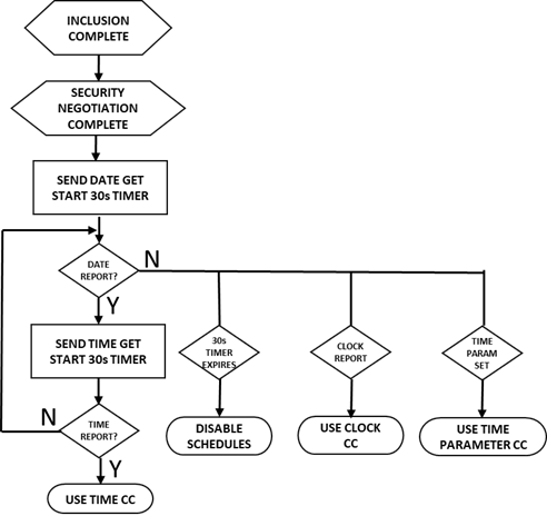
The Low Frequency Crystal Oscillator (LFXO) pins are typically connected to a 32KHz crystal to enable accurate time keeping within several seconds per day. If supporting the Time Command Class, I strongly suggest adding the 32KHz crystal. While you can rely on the LFRCO for time keeping, it can drift by as much as a minute per hour. While you can constantly get updated accurate time from the Hub every now and then, that wastes Z-Wave bandwidth and battery power. Both the Thunderboard and BRD4210 include a 32KHz crystal so you can easily compare the accuracy of each method.
Reserve the EM4WU pins for functions that need to wake the EFR32 from EM4 sleep mode. These are the ONLY pins that can wake from EM4! Note that ports PC and PD are NOT able to switch or input from peripherals while in EM2. See the datasheet and reference manual for more details.
Remaining GPIOs
Many of the remaining GPIOs have alternate functions too numerous for me to mention here. Refer to the datasheet for more details. Most GPIOs can have any of the digital functions routed to them via the PRS. Thus, I2C, SPI, UARTs, Timers and Counters can generally be connected to almost any GPIO but there are some limitations. Analog functions have some flexibility via the ABUS but certain pins are reserved for special functions. Hopefully these tables help you make wise choices about which pin to use for which function on your next Z-Wave product.
Here we go again… Once again I’ve been given yet another board with randomly placed test points instead of a nice neat, reliable header to connect via my MiniSimplicity cable. So I’m spending an hour on my microscope soldering thin little wires to the tiny little test points to be able to flash and then debug the firmware on a new ZG23 based product. Once I’m done soldering, I’m left with a very fragile board which is unreliable at best and at worst will result in even less hair on my thinning head. My post from 2019 described using a zero cost header for a reliable connection, but it seems not everyone is reading my blog!
On the flip side, a different customer sent me their board with a Tag-ConnectEdge-Connect that I had not seen before but is absolutely brilliant. The Edge-Connect uses the EDGE of your PCB for the test points. Barely 1mm wide and about 20mm long it is possible to include this debug connector on virtually any PCB. There is a locking pin to hold the cable secure while the spring loaded tabs press into the castellated notches to ensure solid contact.
Close up of the locking pin and castellated notches
There are several sizes of the Edge-Connect but the recommended one is the 10-pin EC10-IDC-050 which matches the MiniSimplicity header on the WSTK DevKit board. Note that the the 6pin cable in the photo above is NOT the one I would recommend but it was the only one in stock at the time and it worked fine for debugging but doesn’t have the UART or PTI pins.
Tag-Connect has many other types of debug headers/cables of various configurations to hold the cable to the PCB securely. The original Tag-Connect cables have plastic clips that snap into fairly large thru-holes in your PCB. While this is a reliable connection, the thru-holes eat up a lot of PCB real estate. The next evolution was to use a small retaining clip under the PCB that grips onto the metal alignment pins. The photo below shows the PCB pads are not much bigger than an 0805 footprint and only requires three small thru-holes.
Note the smallest header is about the same as an 0805 in lower left corner
The lowest cost approach is to simply add a 10-pin header footprint on your PCB that matches the pinout of the MiniSimplicity header. See section 5.1.1 of Application Node AN958 for the pinout of the 10-pin MiniSimplicity header. You don’t need to solder the header onto the PCB except when debugging. Thus the header can be under a battery or some relatively inaccessible location as when you are debugging in the lab the PCB is usually not installed in the product enclosure.
Please use ANY of these standard connectors on your next project. Without a solid connection between your computer and the chip you will find yourself chasing ghosts and losing hair.
The new Z-Wave 800 Series silicon is now shipping in volume and fully supported by the Silicon Labs tools so it’s time to get to work designing new products! In this post I’ll describe the main advantages and the difference between the chip version (SoC) and the module. But first I want to invite everyone to watch the Tech Talk on using the new 800 series developers kit: ZWAVE-PK800A.
I am presenting the new Z-Wave Developers Kit – ZWAVE-PK800A in a webinar on 22 March 2022. The webinar is recorded so if you missed it, you can still view it anytime, just click the image.
Unlike the 700 series, either the SiP module or the SoC can be used for either controllers or end devices. In the 700 series the EFR32ZG14 SoC is only usable on gateways and only runs the SerialAPI. The ZGM130 module is used for all end devices and can be used on gateways. Thus, the 800 series gives you more choices for which chip/module to use that best matches your product needs.
What’s the difference between 800 series Module vs. SoC?
Here’s the short list of differences:
ZGM230S SiP Module – easier to use
Integrated crystal, RF match, decoupling
Factory calibrated CTUNE
34 GPIO – 44 pin SiP 6.5×6.5mm
+14dBm Max RF Transmit power (lower battery current targeting End Devices)
More expensive unit cost but just add antenna and a few passives
23/31 GPIO – 40/48 QFN 5×5/6x6mm (48 pin compatible with a future larger flash/ram device)
+14dBm or +20dBm Z-Wave Long Range RF Tx power
Line powered devices should use +20 for additional RF Range
Lower unit cost but more companion parts, antenna and crystal calibration required
Both require an external antenna and require regulatory (FCC/CE) testing
ZGM230S Module
The ZGM230S System-in-Package (SiP) Module is a superset of the EFR32ZG23 System-on-Chip (SoC). The module adds a handful of inductors and capacitors for the DC-to-DC regulator and RF matching and the 39MHz crystal which is pre-calibrated at the Silicon Labs factory. The module is easier to manufacture (fewer components and no calibration) but is limited to +14dBm transmit power in Z-Wave Long Range. Modules are more expensive due to the integration but the cost crossover is at pretty high volumes.
ZGM230S SiP Module contains the ZG23 SoC chip, a calibrated crystal and a few passive components
ZG23 SoC
The ZG23 SoC is the chip inside the module. The main advantage of using the SoC is that at high volumes, it is cheaper. The SoC supports +20dBm Z-Wave Long Range transmit power which can nearly double the radio range over the module. But +20dBm demands a lot of battery power so it typically cannot be powered with coin cells but must use a CR123A or AA batteries. Getting FCC to pass at +20dBm can also be a challenge and careful matching of the antenna is required. On the factory test floor, every unit manufactured must have the 39MHz crystal calibrated. Details of the calibration process are described in User Guide 522. The crystal calibration is necessary to ensure reliable radio communication and is a process that requires a spectrum analyzer and several seconds of testing. Your manufacturing partner has to be equipped and knowledgeable to properly calibrate each unit efficiently.
500 vs. 700 vs. 800 Series Comparison
Are you still working with the Z-Wave 500 series and need more details on which series to upgrade to? Fortunately we’ve put together this comparison table to answer those questions. I have to say that once you’ve written and debugged code for a modern ARM processor, you will NEVER want to use the 500 series 8051 8-bit CPU ever again!
Which Z-Wave Series to use?
In these times of long lead times and limited silicon availability, the main question of which Z-Wave chip/module to use may come down to which ones you can get! Silicon Labs keeps some inventory of all of our chips available thru our distributors Digikey, Mouser and Arrow. Each day a few hundred chips of all types are placed into inventory so anyone can buy enough to build prototypes. If there are zero available today, try again tomorrow or the next day. At this time (end of Q1 2022), we are able to supply the 500 series pretty well but the supply outlook for 2023 is uncertain. The 700 series has limited availability so if you already have orders placed and have been given allocation, you are OK. The 800 series is our most advanced process which Silicon Labs and our fabrication partners are investing in upgrading capacity so availability will improve late in 2022 and into 2023. Any new product development or upgrading of 500 series products should use the 800 series. This outlook changesliterally daily so contact your Silicon Labs sales person for the latest recommendation.
Conclusion
The choice of 800 series is easy – do it! The improvements and availability over the 500 and 700 series makes using the 800 series a no-brainer. So the next question is Module or SoC? That decision has to be done on a case-by-case basis as there are a lot of factors to be weighed. The first hurdle is the total unit volume you expect to purchase. If you’re not in the 100,000+ per year stage, then the recommendation is to use the module as it is simply easier to manufacture. The crystal calibration requirement for the SoC is non-trivial and demands expertise and equipment to do it properly. If your target market is not the US, then the module is also the way to go as the additional RF power isn’t available except in the US region as Z-Wave Long Range is only available in North America. I recommend you contact your local FAE to discuss your needs and we’ll help guide to the appropriate solution that balances cost vs. complexity.
Z-Wave is a wireless mesh protocol with over two decades of real-world learning built into the latest version. While the other new wireless protocols are still writing the specification for their mesh network, Z-Wave has learned a thing or two over the past twenty years. Z-Wave is a Source Routing protocol where the Primary Controller of the network keeps track of the best paths thru the network to/from any point to any other point.
Z-Wave limits the number of hops thru the mesh to four hops to bound the routing calculations to something an inexpensive microprocessor can handle. These four hops quickly explode into a huge number of routing combinations as the size of the network grows to more than a few dozen nodes. The trick is to pick the optimal set of routes to get from one node to the next. This is where the two decades of learning have proven to be the key to Z-Waves robust delivery.
Source Routing Introduction
The 500 series Appl. Prg. Guide section 3.4 describes the “routing principles” used in Z-Wave. While this is a 500 series document the 700 series uses the same algorithm with a few minor enhancements. The key to source routing is that the Primary Controller (PC) calculates the route from Node A to Node B. Each node along the way does not need to know anything about the routing, it just follows the route in the packet header determined by the PC. When an end node needs to talk to the PC or any other node, the PC will send the end node four routes to get from Node A to Node B. As a final backup route, Node A can send out an Explorer Frame asking all nodes within radio range if they can help get the message to Node B. If a node is able to help and the message is delivered, this route becomes what is known as the Last Working Route (LWR). Node A will then use the LWR route whenever it needs to talk to Node B.
There are a total of five routes stored in any node to get to any other node. Note that routes are calculated and stored only if a node is Associated with another node. Since most nodes usually only talk to the PC (Associated via the Lifeline – Association Group 1), that is the only set of routes it stores. The primary controller has the full network topology but still follows the same basic algorithm when sending a message to a node. The five routes are held in a list for each destination. If a message is delivered successfully, that route is moved to the top of list and is called the Last Working Route (LWR). The LWR will be used from now on until it fails for some reason. RF communication is fraught with failures and they will happen occasionally so the LWR often changes over time. When the LWR route fails, the list is pushed down and once a working route is found, it is placed at the top of the list as the new LWR.
Application Priority Routes
Application Priority Routes (APR) are special routes the Application can assign to a node to get messages from Node A to Node B. They are called “Application” Priority Routes because the protocol never assigns APRs, only the APPLICATION can assign APRs. Typically the application is the software that is talking directly to the PC – a Hub application like SmartThings or Hubitat or one of the many other Hub applications. The protocol assumes that someone smarter than it (meaning an expensive powerful CPU with tons of memory) can figure out a better route from A to B than it can. The protocol places the APR at the top of the 5 routes in the list and always keeps it there. Even ahead of the LWR. While this gives the application a great deal of power, it also means the application can make a mess of routing and inadvertently cause a lot of latency. Large Z-Wave networks tend to have dynamic routing which is why the LWR has been the key to the routing algorithm – Once you find a working route, keep using it!
PCC Icon for APR
I generally don’t recommend using APRs since the routing tends to be dynamic and it is often best to let the protocol find the best route. However, adding Direct Route APRs where the node will talk back to the Hub directly rather than routing thru other nodes can reduce latency. This sometimes solves the problem where the LWR gets stuck with a multi-hop route when the Hub could reach it directly. A direct route is the fastest way to deliver messages and multi-hop messages often can have noticeable delay to them. When a motion sensor detects motion in a dark room, speed and low-latency are central to maintaining a high WAF factor and quickly turn on a light.
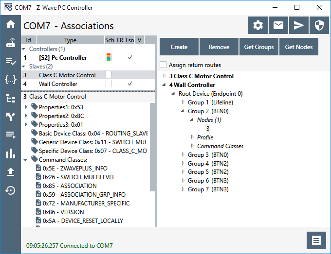
Using the PC Controller to Assign APRs
The PC Controller has a section called “Setup Route” which has a number of ways of setting up various routes.
There are 5 different types of Routes that the PCC can setup:
#
Route
Description
SerialAPI Command
1
Return Route
Assigns 4 controller computed routes between 2 nodes
ZW_AssignReturnRoute() (0x46)
2
Priority Return Route
Assigns an Application Priority Route between 2 nodes
ZW_AssignPriorityRoute() (0x4F)
3
Set Priority Route
Assigns an Application Priority Route from the controller to a node
ZW_SetPriorityRoute() (0x93)
4
SUC Return Route
Assigns 4 controller computed routes from the end node to the controller
ZW_AssignSUCReturnRoute() (0x51)
5
Priority SUC Return Route
Assigns an Application Priority Route from the controller to an end node
ZW_AssignPrioritySUCReturnRoute() (0x58)
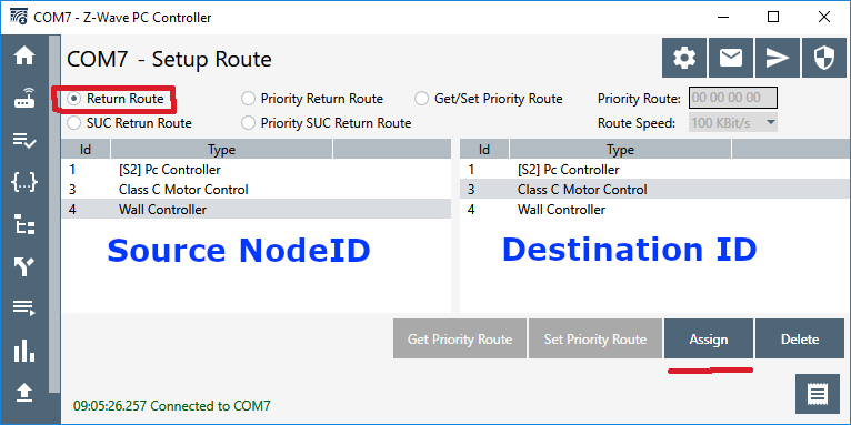
1. Return Route
Return Route assigns four routes to the source node (left) to reach the destination node (right). Anytime an Association is made from one node to another, a Return Route MUST be assigned so the source knows how to reach the destination. The most common application is a motion sensor turning on a light without going thru the hub. For example; a motion sensor (Node 10) is associated with the light (Node 20) and then a call to ZW_AssignReturnRoute(10,20,SessionID) will send four messages to node 10 with four different routes to get to node 20. In this case the Application does NOT specify the route to be used but lets the Primary Controller calculate the best 4 routes. The source node can still use Explorer Frames to find a route if all four fail. During inclusion a controller should always assign return routes to the end node back to the PC so the end node has routes for any unsolicited messages (or use the SUC Return Route below). If the network topology changes significantly (nodes added or removed), then all the return routes of every node in the network should be reassigned to ensure the optimal route is used.
2. Priority Return Route
Priority Return Route is used to assign an Application Priority Route between two nodes. The only time I recommend using this command is to assign a priority route back to the controller to use no routing assuming the node is within direct range of the controller. It is too easy to mess up the routing with this command so in general I do not recommend using it.
3. Get/Set Priority Route
Get or Set the Application Priority Route (APR) the primary controller uses to reach a node. Since the node will use the same route to return the ACK this will become the LWR for the end node so both sides will use this route first. Note that this route is not set at the end node, only the controller will use this route. If the end node needs to send a message to the controller it will use this route if it is the LWR otherwise it will use one of its own assigned routes. Note that you can set the speed in this command. Be careful not to blindly set the speed to 100kbps. If the nodes in the path are older or the destination is a FLiRS device then they may only support 40kbps. Old 100 series nodes can only do 9.6kbps but they can still be part of the mesh. Note that you can GET the priority route (0x92) with this command if one has been assigned. If a Priority Route has not been assigned then the current LWR is returned.
The only application of Set Priority Route I recommend is to force nodes close to the controller to always try direct communication first. In this case, you would Set Priority Route with all zeroes in the route. This tends to make scenes that turn on a lot of lights run quickly so there is less popcorn effect. If a scene with a lot of lighting nodes fails to deliver to one of the nodes, the PC then searches thru routes to find a new route, the routed route becomes the LWR and the controller will continue to use the LWR until that route fails for some reason. By assigning a Priority direct route the controller will always try the direct route first. Since 700 series devices usually have excellent RF, if the controller is in the same room or at least on the same floor as the lights it is controlling, then the direct routes will minimize the popcorn delay. However, if the lights are not in direct range, it will just delay everything making the popcorn worse! So be careful in assigning APRs! Don’t make things worse.
Set the Application Priority Route to Node 2 to direct (no hops) at 100kbps
The example above shows how to assign an APR direct route to Node 2. The function call for this would be: ZW_SetPriorityRoute(2, 0, 0, 0, 0, 3); Every time the PC sends a message to node 2 it will always try this direct route first, if that fails to ACK, then it will use the LWR then the other return routes it has calculated.
APR to Node 6 thru 5->4->3->2 at 100kbps
The example above shows an extreme example where we force routing to be the maximum number of hops of four. This is a handy way to test your product with a lot of routing! A zniffer trace of a message looks like:
Node 1 sending Basic Set to Node 6 via 1->5->4->3->2->6
The function call for this would be: ZW_SetPriorityRoute(6, 5, 4, 3, 2, 3); The PC will always use the route to send a message to node 6, if it fails, it will try the LWR and then the other return routes and finally an Explorer Frame.
4. SUC Return Route
The SUC Return Route is a shorter version of the Assign Return Route (1. above) which simply sets the Destination NodeID to be the SUC which in most cases is the Primary Controller.
5. Priority SUC Return Route
The Priority SUC Return route is again a short version of the Assign Priority Return Route (2. above) which automatically sets the Destination NodeID to be the SUC. It is generally easier to simply use the normal Return Route commands (1. aan 2. above) and fill in the Destination NodeID as the PC (which is usually the SUC) than to use these two commands.
Conclusion
The techniques explained here are not intended for general Z-Wave users but instead for the Hub developers and end-device developers. Since these are low-level commands and not something a user typically has access to, you’ll have to pressure your Hub developer to follow these recommendations.
Hub developers MUST assign return routes ANY time an Association is made between two nodes especially back to the Hub immediately after inclusion and assignment of the Lifeline. If the network topology changes such as when a node is added or removed, it may be necessary to reassign ALL of the routes to all nodes to take advantage of the new routes or eliminate nodes that no longer exist. Be careful assigning Priority routes especially if a node in a Priority Route is removed from the network. If a now non-existent NodeID is in an APR, the node will try really hard using the APR with the missing node before finally giving up using the LWR. This will result in annoying delays in delivering commands or status updates. Z-Wave will still deliver the message, but only after you’ve banged your shin into the coffee table in the dark because the motion sensor is still trying to send thru the missing NodeID in the Application Priority Route.
All wireless protocols can be jammed often using an inexpensive battery powered transmitter. The protocol doesn’t even have to be radio frequency (RF) based as Infra-Red (IR) and any other communication medium that travels thru the air can be jammed by blasting out noise in the same spectrum as the protocol. Think of a busy street corner where you and a friend are having a conversation and a firetruck with their sirens blareing go by. Your conversation stops because your friend simply can’t hear you above all the noise. The same thing can happen in Z-Wave where a “bad actor” brings a small battery powered transmitter and blasts out RF in the same frequency bands that Z-Wave uses. In this post I’ll explain how to jam Z-Wave and also how to detect and inform the user that jamming has occurred.
Security System Requirements
Jamming applies primarily to security systems. After all, if someone wants to jam your house from turning on the kitchen lights at night, what’s the point other than to get a laugh when you bang your knee into the table? Z-Wave has enjoyed a great deal of success in the security system market. Z-Wave is interoperable, easy to use, low-power and the mesh networking protocol means users or installers don’t have to be concerned with getting everything to talk to everything else as the protocol automatically handles (mostly) everything. Security systems however are very concerned about jamming to the point that Underwriters Laboratory has a specification for it. UL1023 is the US standard for Safety Household Burglar-Alarm Systems.
The reality of the situation for a security system is that it is unlikely a burglar will try to bypass your security system by jamming it. Burglars are simply not that tech savvy. The FBI doesn’t even track the numbers of burglaries via jamming – one would assume because the number is essentially zero. A burglar will simply bash in a window or door or more often simply walk in an unlocked door. However, if it’s easy enough and cheap enough, a burglar might just try! CNET demonstrated just how easy it is to use a $3 transmitter to bypass a popular security system using a cheap RF transmitter. Regardless of the reality of the situation, the bad press of having an easy to jam security system can crater a company.
Anti-Jamming Techniques in Z-Wave
Z-Wave was designed from day one to be robust and reliable. The very first requirement for robustness is to acknowledge that the device receiving the message did in fact receive it. Every Z-Wave message is acknowledged (ACK) otherwise the sender will try again using different mesh routes or other RF frequencies. After several retries, the protocol will give up and the application can then decide if it wants to try even more ways to deliver the message. If the message is not very important (like a battery level report), the application can just drop it. If a sensor detects smoke! Then the application will continue trying to get this life-safety message thru in every way possible for as long as possible.
Z-Wave requires two-way communication – all messages are acknowledged
Here’s a list of the techniques Z-Wave uses for robustly delivering messages:
Z-Wave
All frames are Acknowledged
Multiple mesh routes
Frequency Hopping – Two frequencies – 3 different baud rates (in US)
RSSI Measurements indicating jamming
Supervision CC confirms decryption & data integrity
Z-Wave Long Range
All frames are Acknowledged
Dynamic TX Power
Frequency hopping to alternate channel
RSSI Measurements indicating jamming
Supervision CC confirms decryption & data integrity
Even with all these different measures in place, it is still possible to jam Z-Wave. But it’s not cheap nor is it easy. But let’s give it a try for fun!
Jamming Z-Wave
Jamming Z-Wave starts with a Silicon Labs Z-Wave Developers Kit and Simplicity Studio. However, these kits are not cheap costing at least $150 for just one. It may be possible to find a cheap 900MHz transmitter but you will need two of them and they must have the ability to tune them to the specific Z-Wave frequencies of 908.4MHz and 916MHz in the US. These are not going to be $3 battery powered transmitters and they require a significant amount of technical knowledge. Neither cheap nor easy so I think we’re pretty safe from your typical burglar.
Z-Wave uses two channels (frequencies) in the US: 908.4MH for 9.6 and 40Kbps and 916MHz for 100Kbps. Z-Wave Long Range (ZWLR) also has two channels but uses spread-spectrum encoding which spreads the signal out across a band of frequencies centered at 912MHz and 920MHz. By using two channels Z-Wave is frequency agile which makes it harder to jam since you need two transmitters instead of just one. The spectrum analyzer plot below shows four DevKits blasting all 4 channels at once.
Z-Wave jamming all four frequencies – 912 & 920 are Z-Wave Long Range
Creating the jammer firmware utilizes the RailTest utility in Simplicity Studio V5. Select the DevKit in the Debug Adapters window, click on the Example Projects & Demos tab then check the Proprietary button. The only example project should be the “Flex (RAIL) – RAILtest application”. Click on Create and use the defaults. The default frequency will state it is 868 but ignore that as the Z-Wave modes are all built into RailTest and do not need to be configured. Once the project is created, click on Build and then download to a devkit. Right click on the devkit in the Debug Adapters window and click on Launch Console. Click on the Serial 1 tab then click in the command box at the bottom and press ENTER. You should get a RailTest prompt of >.
Once you're at the RailTest prompt, enter the following commands:

rx 0                 -- disables the radio which must be done before changing the configuration
setzwavemode 1 3     -- Puts the radio into Z-Wave mode
setpower 24 raw      -- 24=0dbm radio transmit power - valid range is 1 to 155 but is non-linear
setchannel 0         -- ch0=916 ch1=908.4 ch2=908.42 - ZWLR ch0=912 ch1=920
setzwaveregion 1     -- EU=0, 1=US, 13=US Long Range
Do one of the following 2 commands:
SetTxTone 1          -- narrow band Carrier Wave - unmodulated
SetTxStream 1        -- Pseudo-Random data - modulated and in ZWLR uses Spread Spectrum (DSSS)
Use the same command with a 0 to turn the radio off
Remember to "rx 0" before changing any other configuration values
RAILtest is a powerful utility and can do all sorts of things beyond just Z-Wave. The radio in the Silicon Labs chips are Software Defined Radios, they can be customized to many common frequency bands. It is easy to create customized versions of RAILtest that will transmit a carrier wave (CW) or a modulated signal at just about any frequency band, not just Z-Wave. But that’s more complex than I have time to discuss here.
Now that we know how to jam, how do we detect it and inform the user that jamming is taking place? Detecting jamming takes place at both ends of the Z-Wave network, the Controller and the End Device. Let’s first look into the End Device which in a security system is typically a motion sensor or a door/window sensor.
End Device Jamming Detection
Most end devices are battery powered so they spend most of their time sleeping and are completely unaware of any RF jamming that might be taking place. Only when motion is detected or a door is opened will the sensor wake up and find the radio waves being jammed. The best way to check for RF jamming is to first try to send a message. When the message fails to be acknowledged, then start looking to see if jamming is occurring.
The Z-Wave Application Framework (ZAF) handles sending the message and eventually calls a callback to report status. The callback comes through EventHandlerZwCommandStatus() which will be called several seconds after sending the message. The protocol tries various mesh routes, power levels and baud rates which takes time so be sure to stay awake long enough to receive the callback. The callback returns the TxStatus variable which is typically TRANSMIT_COMPLETE_OK (0x00) which means the message was delivered. But if jamming is taking place and the radio was unable to go through it, you’ll get a TRANSMIT_COMPLETE_FAIL (0x02). This status is different than the TRANSMIT_COMPLETE_NO_ACK (0x01) which means the message was not acknowledged which is usually because the destination is offline but could also be due to jamming.
The next step is to verify that jamming is taking place by getting the current Received Signal Strength Indicator (RSSI) level by queuing the EZWAVECOMMANDTYPE_GET_BACKGROUND_RSSI event . The RSSI is a simple value in dB of the strength of signal at the radio receiver when its not actively receiving a frame. In normal operation, this value should be around -100dB. Every environment is different so the threshold for the radio being jammed needs to be a value that is significantly higher than the average value. This is particularly tough in dense housing like apartments where perhaps every unit has a Z-Wave network. This results in a relatively high RSSI average. The key here is you can’t use a simple hard-coded threshold for jamming detection based on RSSI. Instead you must average the RSSI values across a long time-span (typically hours).
Z-Wave Notification of Jamming
The next step after detecting jamming has occurred is to notify the hub. But if the jamming is still in progress, how can the notification get thru? Naturally you can’t get thru while the jamming is still happening. The trick is to keep trying and hope that the jamming is short term. The problem is that a battery powered sensor can’t keep trying constantly as it will run out of battery power perhaps in just a few minutes. You must manage battery power and at the same time keep trying with a longer and longer timeout between attempts. At some point the jamming should end, perhaps hours after the initial break-in but the jammer will eventually run out of battery power.
The Z-Wave Notification Command Class has a pre-defined value for RF Jamming – Notification Type of Home Security (0x07) with an Event of RF Jamming (0x0C) and the current average RSSI level. This notification is a critical notification so it should be wrapped in Supervision Command Class to guarantee it has been delivered and understood by the controller.
Sample Code
The code below first checks the TxStatus, if is not OK, then the RSSI level is checked by queuing the GET_BACKGROUND_RSSI event. Once the RSSI is sampled, the function will be called again with the switch going thru the GET_BACKGROUND_RSSI case below. This section of code then compares the current RSSI level with a background RSSI level and if the current level is above it then the SendRFJamNotificationPending global variable is set. When a frame is able to get thru then the pending RF Jam notification is sent since it appears the jamming has ended. This ensures the Hub is informed that there was jamming so the Hub can then decide if it needs to inform the user. The basics of the algorithm are coded here:
...
static void EventHandlerZwCommandStatus(void)
...
switch (Status.eStatusType)
...
    case EZWAVECOMMANDSTATUS_TX:  // callback from attempted message delivery
...

        if (pTxStatus->TxStatus != TRANSMIT_COMPLETE_OK) { // failed to deliver - check RSSI
            EZwaveCommandType event = EZWAVECOMMANDTYPE_GET_BACKGROUND_RSSI;
            QueueNotifyingSendToBack(g_pAppHandles->pZwCommandQueue, &event, 0); // Queue GET_RSSI
        } else { // message delivered OK
            // more cleanup happens here...
            if (SendRfJamNotificationPending) { // Is there a pending Jam Notification?
               SendRfJamNotificationPending=false;   // Send it!
               void * pData = PrepareNotifyJamReport(&zaf_tse_local_actuation);
               ZAF_TSE_Trigger((void *)CC_NotifyJam_report_stx, pData, true);
            }
        }
...
    case EZWAVECOMMANDSTATUS_GET_BACKGROUND_RSSI:  // only called if failed to deliver a message
        if (Status.Content.GetBackgroundRssiStatus.rssi > BackgroundRSSIThreshold) {
            // Set a global to send an RF Jamming Notification which will be sent when jamming ends
            SendRfJamNotificationPending=true;
            SendRfJamNotifRSSI= Status.Content.GetBackgroundRssiStatus.rssi;
        }
... // Not shown are application level retries and various other checking
Now that we have jamming detection enabled on the end-device side, let’s look at the controller end of the communication.
Controller Jamming Detection
Obviously the main thing the controller needs to do is react to a jamming notification from an End Device. The ultimate action the controller performs is left to the controller developer but clearly the end user should be notified that jamming has been detected. But that notification needs to be qualified with enough information about the average RSSI noise level to avoid false jamming detection notifications.
If the jammer is way out at 200+ meters, the RSSI level may not jump up significantly as measured by the controller. Thus, it is important to react to the End Device notification of jamming. However, the controller must poll the RSSI level at regular intervals to determine if jamming is taking place nearby. The question is how often should it poll and when to react to a sudden change in the RSSI level? There is no definite answer to this question other than “it depends” and it depends on a lot of different factors. Typically, the RSSI should be sampled a few times per minute – perhaps every 30 seconds. If a value seems unusually high, perhaps sample several more times at a much faster rate to confirm that the RSSI has jumped and its not glitch. Like the End Device case, the average RSSI value needs to be calculated across a fairly long time frame (minutes to perhaps an hour) and when there is a change from the average value then the user should be notified.
ZW_GetBackgroundRSSI
The SerialAPI function ZW_GetBackgroundRSSI() (0x3B) will return three or four bytes of RSSI values for the various channels supported by the controller. This function can be sent to the Z-Wave controller frequently as it does not cause any delays in the radio. It does use UART bandwidth so it can’t be called too frequently or it may interfere with normal Z-Wave traffic. The polling function should coded with a low priority so it is only sent when the UART has been idle for a few seconds to avoid collisions with Z-Wave radio traffic. The one-byte RSSI values are coded as shown in the table below.
RSSI values returned by the ZW_GetBackgroundRSSI():
Hex
Decimal (2s Comp)
Description
0x80-0xFF
-128 – -1
Measured RSSI in dBm
0x00-0x7C
0 – 124
Measured RSSI in dBm
0x7D
125
RSSI is below sensitivity and cannot be measured
0x7E
126
Radio saturated and could not be measured as it is too high
0x7F
127
RSSI is not available
Typically a 700 series Z-Wave controller will measure about -100dBm when the airwaves are fairly quiet. During a transmission the RSSI is often about -30dBm when the node is within a few meters of the controller.
TxStatusReport
The TxStatusReport is returned after a frame was transmitted which includes several fields with a variety of RSSI measurements. There is a Noise Floor of the sender as well as a NoiseFloor of the receiver. The RSSI values can be monitored during normal Z-Wave traffic without polling. It is best to use these values while Z-Wave traffic is taking place and to temporarily pause the polling while the Z-Wave UART is busy. Once the UART is idle, resume RSSI polling.
Missing Heartbeats
Another aspect of jamming is that battery powered devices typically send a “heartbeat” message every hour so the controller knows for sure the device is online and working (mostly that the battery isn’t dead). The controller should be keeping track of how long it has been since the last time a battery powered node has checked in and if it has missed two or at most three heartbeats, the controller should inform the user (or the installer) that the device is offline and unable to communicate. If the battery was already low, then the battery is probably dead. If the battery was fine, then there is a possibility that the device is being jammed.
The Jasco Motion Dimmer is an ideal Z-Wave product for home automation. We want the lights to come on automatically when we enter a room and off again when everyone has left. The motion sensing needs to be reliable and sensitive and ideally not involve changing batteries every few months. Thus, a wall mounted, always-on dimmer with a built-in motion sensor fits our needs perfectly. In this blog article I’ll explain a few tricks to getting the most out of this handy device.
Configuration Parameters
The Jasco Motion Dimmer has 18 configuration parameters. The parameters can be set by reading the documentation and then programming them using complex combinations of button presses. But, with a Z-Wave device, it’s much easier to program them via Z-Wave. Most Hubs allow you to program the configuration parameters though the process to do so is different with every Hub. The parameters are briefly described on the Jasco web site ezzwave and on the Z-Wave Alliance web site. However, these brief descriptions don’t clearly describe what the parameter does and more importantly, what the best settings are to get the most out of this device.
Several parameters are two bytes instead of just one even though the value will typically fit in one (the value is 0-255). The parameters listed with a (2) in the Name field below means they are two bytes. If there is no (2) in the name then just send one byte. Sending just one byte to the 2 byte parameters can confuse the dimmer and it may not set the parameter to the desired value. The result is frustration as you sent it your desired value but it didn’t take it or set it to what appears to be some random value. Always send the proper number of bytes for each specific parameter. Some Hubs will handle this for you, but others must be done manually.
The table below is the list of all parameters with the less important ones greyed out and my own more detailed description of what each parameter does.
#
Name
Default
Description
1
Timeout
5
Motion Sensor Timeout 0=5s test mode 1-254=minutes 255=disable Time the lights remain on in Occupancy mode
2
Assoc dim
255
0=99 dim level 255=last ON level Dim level to send to associated lights. The Hub is better at controlling other lights so ignore this parameter.
3
Mode
3
1=Manual – Motion sensor does not control the local load 2=Vacancy – only turns lights off 3=Occupancy – Lights on when motion detected and off when none after Timeout
4
Invert buttons
0
0=normal (top=up, bottom=down) 1=invert (top=down, bottom=up) If you accidentally install the dimmer upside down, inverting it will correct your mistake
6
Motion Enable
1
0=disable 1=enable Why would you disable motion sensing?
7
Steps via Z-Wave
1
Leave at 1 See the Ramp Rate discussion below
8
Speed via Z-Wave (2)
3
Number of seconds for the dimmer to go from 0 to 100% via a Z-Wave command
9
Steps via button
1
Leave at 1
10
Speed via button (2)
3
Number of seconds for the dimmer to go from 0 to 100% via a button press or the motion sensor
11
Steps via AllOnOff
1
AllOnOff commands are obsolete
12
Speed via AllOnOff (2)
3
Leave at default
13
Motion Sensitivity
2
1=high – detects people at a distance 2=Medium 3=low – less likely to detect a pet
14
Light Sensing
0
0=disabled 1=enabled If enabled and the room is brightly lit the lights will not turn on when motion is detected
15
Reset Time (2)
2
0=disabled 1=10s, 2=20s, 3=30s, 4=45s, 5-255=n*15s When Motion is detected a notification is sent to the hub saying there is motion. After Reset Time, a reset notification to clear the motion event is sent. If you are still in the room, motion and reset notifications will continue to be sent. Depending on your hub you may want to change this but generally the default works.
16
Switch Mode
0
0=disabled 1=enabled Switch mode changes the dimmer to act like a switch so the light turns on (100%) or off instantly. If you want this mode, buy the cheaper switch instead.
17
Switch Level
0
0-99=Brightness level Sets the dim level when motion is detected or the top button is tapped. You can press and hold the top which will continue to increase the dim level further if you have set this to something other than 99. Ignored when Switch Mode is enabled.
18
Dim Up rate
0
0=fast 1=slow This applies only to commands sent via Z-Wave and only applies to the dim up ramp rate. Best to leave this at the default of 0 and use parameters 8 and 10 instead.
19
Exclusion Mode
0
0=any button 1=Tap X then ON will enter exclusion mode, Tap X then tap OFF 10 times in less than 5 seconds will factory reset the dimmer. X is the little button behind the face plate to the left of the ON button. Enable this mode if there are other Z-Wave networks nearby (IE: in a condo or apartment) to reduce the risk that one of these other networks will exclude the dimmer when you tap one of the buttons. When 0, every time you tap either On or Off the NIF is sent. If a nearby controller is in exclusion mode, your dimmer will be excluded from YOUR network and it will seem to stop working. I recommend setting this to 1 either way to reduce the chance even within your own household of accidentally excluding the dimmer.
Configuration Parameters
Dimming Ramp Rates
When a dimmer changes the light level from 0 to 100%, the time it takes for the light to go from 0 to 100% is set by the Ramp Rate. The dimmer has six parameters related to the dimming ramp rate, parameters 7 through 12. The ramp rate is configured using a pair of parameters for three different methods of changing the light level. The “Steps or Levels” is the number of dim levels that the light level changes every Time Step. Always leave the Steps at the default of one. Anything more than one results in the light level “jumping” from one step to the next while dimming. This jumping is just plain unpleasant so always leave Steps at one. The Time Step parameter (Speed) is how often the Step is added to the current dim level in 10 millisecond increments or every 1/100th of a second. Since the dim level goes from 0 to 100 and it takes 1/100th of a second to increment once, then the Time Step simply is the number of seconds for the dim level to go from 0 to 100%. The default ramp rate is three seconds which is what most people expect and in general is a good value.
The three pairs of ramp rates provide different ramp rates based on the method to turn the light on or off.
Z-Wave command – parameters 7 and 8
Button or Motion detection – parameters 9 and 10
All On/Off commands – parameters 11 and 12
The easy ones to ignore are the All On/Off parameters as the Z-Wave All On/Off commands are obsolete. Simply leave these at the default. The remaining two pairs can be used for different purposes based on what is changing the light level. I recommend leaving the Button/Motion parameters at the default of 3 seconds. This is the expected ramp rate of the average dimmer. When a person presses the button or motion is detected, they expect the dimmer to react at about this speed. Setting it to less than 3 seconds results in the user being unable to set a mid-level as the ramp rate is too fast to accurately stop at a mid level. The dimmer pretty much becomes a switch. Setting the ramp rate to more than 3 seconds will quickly become annoying as it just takes too long to get to the desired level. That leaves the Z-Wave command ramp rate parameters. These can definitely be programmed to be longer, potentially much longer so that the level changes quite slowly and an occupant can override the slowly changing light level by pressing the button or waving their hands in the air so the motion sensor will detect them.
The Z-Wave Multilevel Switch command Version 2 includes a Duration field which is the number of seconds to go from 0 to 100% or the ramp rate. If the Hub sends a dim level command with the Duration field, the configuration parameters are ignored and instead the ramp rate is set to the Duration value in the command. Some Hubs let you assign the Duration field but most only support Version 1 which only has the level and no duration which the dimmer will then use the configuration parameters dim rate.
Association Groups
Three association groups are supported with up to five NodeIDs each. Your Hub should automatically assign itself to Group 1 which is the Lifeline group. The Lifeline group is required for every Z-Wave Plus device and identifies the NodeID where any state changes will be sent. The dimmer sends your Hub commands whenever the sensor detects motion or the state of the local load changes (someone presses the On or Off button). Thus, it is very important that the Hub be assigned to Association Group 1 so Hub app on your phone matches the actual state of the dimmer.
Groups 2 and 3 are identical and simply send Basic On/Off commands to the associated NodeID. Assigning a NodeID to these groups will send a command to turn the NodeID either On or Off when motion is detected or not. Assigning a NodeID to these groups enables the motion detector or the buttons to turn on/off other lights in a larger room quickly. Using the association groups is fast since the dimmer sends the Z-Wave commands directly to the light and works even if the Hub is offline for some reason.
Multi-channel associations are supported but generally you want to avoid them. Multi-channel adds another layer of encapsulation to every frame which just slows everything down. The only time you might want to use multi-channel association is if you wanted to control a specific outlet in a power strip with the motion sensor. Multichannel would be required to choose which of the outlets in the power strip to turn on/off. However, I recommend that you let your Hub do complex operations like this and keep things simple with the dimmer.
Group
Name
Description
1
Lifeline
Motion Sensor readings and status of the load are reported
2
Basic On/Off
BASIC SET On or Off commands
3
Basic On/Off
BASIC SET On or Off commands
Association Groups
When a NodeID is assigned to an association group, the node will be interviewed and depending on the command classes the node supports, the dimmer will send different commands. Specifically, if the device supports CRC16 then the commands will be encapsulated in CRC16 which improves the reliability of the command being delivered without errors but isn’t really necessary.
Why are there two association groups you ask? The reason is to match the feature set of many other Jasco Z-Wave products which send different commands in the two groups. But for this device it always sends the same commands from either group. My recommendation is to not use Group 3 at all. If you want to associate other lights directly with the dimmer, use Group 2.
Recommendations
There are many ways to use a motion sensor wall dimmer. Perhaps the toughest question is where to install it? The first place I installed my motion dimmers are in hallways. When your arms are full of groceries, you want the lights to just come on when you enter. More important in my household is that the lights go OFF shortly after everyone has left the hallway! Back in the bad ol’ days, the hallway lights were always on all the time because no one ever turned them off! The challenge with hallways is typically they are 2, 3 or more way lights so the placement of the motion sensor is key. Jasco makes an inexpensive Add-On Switch that connects to the Traveler wire to enable the multi-way switch so it can be operated manually as before. However, getting the motion sensor to cover a long thin hallway can be difficult since the motion sensor is built into the wall and cannot be pointed down the hallway. In that case you may need to use a separate battery powered motion sensor to trigger normal dimmer switches. What this means is that a wall mounted fixed position motion sensor may not work for all situations but the sensor has a wide angle lens so it will work most of the time.
Easy Mode – Use the Defaults
The simplest configuration is to use the dimmer as-is using the default settings. The defaults work as you would expect and obviously is the easiest to setup and use! Perhaps the only real decision here is which wall switch to replace. In this mode the lights come on when motion is detected and off after 10 minutes. Perhaps the one configuration to adjust would be the Timeout especially for hallways. Since you’re usually passing thru the hallway and thus moving quite a bit, the Timeout can be short, one or two minutes. A short Timeout keeps the power consumption to a minimum while providing sufficient light to travel thru the space.
Slow Dim – Parameter 8
The next parameter to consider customizing is the Z-Wave dim ramp rate (Parameter 8). The motion sensor and the buttons continue to use the typical 3 second ramp rates which are what people would normally expect. But when a Z-Wave command sends a command to change the light level, a significantly slower ramp level can be used. This configuration lets the user override the dim level either by moving or pressing a button. The slow ramp can be 30 seconds in this mode or perhaps as short as 10s. This always gives the person in the room time to override the slow dim but still provide enough light to move around the room as needed. The most common case for this is in a room where people might be reading, watching TV or working on a computer where they are not moving very much.
Manual Mode – Parameter 3
Configuration Parameter 3 has three different settings. The default is Occupancy mode which is the most useful and common mode. Vacancy mode only turns the light off but you have to manually turn it on – don’t bother with this mode. The third option is Manual mode which disconnects the motion sensor from the local load. Your Hub has to then turn the light on when the motion sensor detects motion. The time from motion detection to the light coming on has just a little more delay but often this delay isn’t that much. What you gain from this setup is a great deal more flexibility in how the lights should dim up or down.
My Setup
The first motion dimmer I installed was in my mudroom which is pretty much a hallway with a closet but it is an L shape. It is a 3-way switch with wall switches at each of the 3 entrances. Fortunately the switch with the incoming power is the one with the best view down both legs of the L and is where I mounted the motion dimmer. I use Easy Mode in this situation since the desired operation is quite simple. You walk in, the lights come on, you leave and 10 minutes later the lights go off. I suppose I should shorten the Timeout but I’ve never been in the mudroom and had to waive my hands to turn them back on even when rummaging thru the closet where the motion sensor can’t really see me. If I made the timeout shorter, then the lights might go off before I’ve found what I’m looking for. Nothing craters the WAF Factor more than the lights turning off before my wife has found what she’s looking for in the closet!
The next one I installed is in the garage. In this case I used a Motion Switch rather than a Dimmer since its a few bucks cheaper and I don’t need a dimmer in the garage. Easy Mode is fine in this situation. I have a 2 car garage about 24′ square and the motion sensor is able to detect motion of a person just about anywhere in the room even though the wall switch is in the corner next to the door into the mudroom. I did change Motion Sensitivity (Parameter 13) to high to get the entire garage to detect motion. I also enabled Light Sensing (Parameter 14) as my garage has quite a few windows and has plenty of light during the day. There is no way to adjust the level of light to disable the light from turning on but it seems to work when I want it to and doesn’t turn on the lights when the room is sufficiently bright from natural sunlight.
My master bedroom closet seemed like a simple setup but took a little more tweaking. What I want is the light to come on at a low level (say 5%) but if it’s daytime or early evening I want the light to come on fully. With this setup the light is just enough to find my robe in the middle of the night without waking my wife but she can choose an outfit in full illumination. Since the dimmer has no idea what time of day it is, I need to enlist the help of my hub. I set the Switch Level (Parameter 17) to 5% and the Z-Wave Dim Rate (Parameter 8) to 30 seconds. Then I created an event on my hub (Homeseer) that sends an ON command whenever motion is detected and the time is between sunrise and 9pm. This ON command will take 30s to come on fully which is nice. Since the Button Dim rate remains at 3s the buttons operate as normal so if my wife is impatient she can press the top button to quickly get the lights fully on.
My kitchen is the most complicated setup by far. First of all, I have an eat-in kitchen which is pretty wide and the dimmer often doesn’t detect if we are sitting at the table which is at the end of the kitchen. The Jasco Motion sensor is mounted basically in the middle of my kitchen and there are a variety of kitchen appliances on the counter blocking the view of the kitchen table. To cover this wide space I enlist a second motion sensor that is close to the table so even if someone is sitting there quietly, perhaps reading, the combination of the two sensors ensures that the lights only go off when no one is there (most of the time). I use Manual Mode (Parameter 3) in this case and rely on my Hub to combine the 2 sensors readings and control the lights appropriately. Manual Mode effectively disconnects the Jasco Motion Sensor from the Dimmer. When either motion sensor detects motion, I set the dimmer to full on. When BOTH motion sensors have not detected motion for about 20 minutes, then I turn the dimmer off. By relying on the smarts of my Hub I can do even more interesting events where the timeout is different late at night when someone is probably just passing thru and I can use a lower dimmer level. At meal times I push the dimmer fully on as we’re probably preparing food so the more light the better. I could even check for the light level provided by the windows in the room and then only add as much illumination as needed though I haven’t experimented with this yet.
Conclusion
Once you have a few lights automated, you’ll almost never touch the buttons. The lights come on when you walk in and off when everyone leaves. Your family quickly becomes used to it and it blends into the woodwork which is the way things should work. Adding motion sensor lights to your home is an incremental upgrade. I suggest starting with your most-used light such as a hallway or mudroom. Once the family has adjusted to one, you can add more in other locations as the budget allows.
The Jasco Motion Dimmer is a versatile and invaluable home automation device. Never needs batteries and is configurable enough to handle even fairly complicated situations. The trick is to use the right tool for the job. The dimmer is fine for basic operation but use the smarts built into your Hub to do more complicated tasks. Being highly configurable unfortunately results in more complexity but I hope my guide helps you make the most of this device. Let me know what you think and any other Z-Wave related topics you’d like to discuss in the comments below.
Frequently Listening Routing Slaves (FLiRS) are a class of Z-Wave devices that are battery powered but wake up every second to check if there is a message waiting for them. FLiRS were initially used for door locks. Door locks have fairly large batteries since they have to move a mechanical device to lock or unlock a door. Typically this is four AA batteries. With this fairly large battery storage, we still need a method to talk to the lock but can’t stay awake all the time as the batteries would only last a week or so. FLiRS to the rescue! FLiRS lets the lock remain asleep 99% of the time and wake up very briefly once per second and listen for an always-on device to be sending a “Wakeup-Beam”. The Beam is a constant transmission of the NodeID and a 1 byte hash of the HomeID telling that specific node to fully wake up and be ready to receive a message. This low-power mode allows Z-Wave devices to run for years on a battery but still be ready to lock or unlock within 1 second.
Z-Wave door locks first appeared in 2008 but since then FLiRS mode has found uses in other battery powered devices. The next most popular FLiRS device are thermostats. Older heating systems which rely on a simple mercury switch have only 2 wires and do not need power. To upgrade these simple switches to a smarthome Z-Wave thermostat means a battery powered device has to last for years on a single set of 3 or 4 AA batteries. FLiRS to the rescue again! Since a user is fine if it takes a few seconds to change thermostat settings, FLiRS is the ideal way to extend battery life and still be connected to the internet.
Recently we’ve had a number of window shades come to market based on FLiRS. Window shades have the challenge that often there is no power near the window so they need to be battery powered. Sometimes a solar cell can help keep the batteries fresh but the FLiRS mode is key to long battery life. Controlling the shades with Alexa is the favorite mode to show off your smarthome – “Alexa, set shades to 0%”. The challenge comes in if you want a battery powered wall switch or some other device to directly control the shades. This is usually done using a Z-Wave Association where the wall switch is “associated” with the shade and then controls the shades without the Hub being involved. This is faster and in some cases can be done without a Hub at all. The trick is getting the wall switch to send the Beam to wake up the shades. Setting the Association is insufficient. A Return Route has to be sent which will tell the wall switch to send a beam.
Association
The first step in directly controlling the shades from a wall switch is to assign the shade to an Association Group. Using the PC Controller application to add the association is done by selecting the destination in the left window and then choosing the Association Group to add it to in the right window. In this case I’ve added the shade NodeID=3 to the Wall Controller NodeID=4 Group 2 which will send a BASIC_SET when I press button 0.
Note the checkbox for Assign Return Routes. Initially I’ll leave this unchecked. This is what many Hubs fail to do properly – set the Return Route anytime an association is made. So what happens when I press Button 0?
The Wall Controller (nodeID=4) sends the Basic Set command 3 times but the Shade (nodeID=3) does not ACK. The Wall Controller tries two more time with Explorer Frames trying enlist anyone else in the network to deliver the frame. But they all fail. Why? Because the Shade is asleep waiting for a Wakeup Beam.
Assign Return Route
To get the Wall Controller to send a FLiRS Wakeup Beam we have to tell it to send one! That is done by assigning a Return Route. In the PC Controller the easy way to do that is to simply check the box in the Association window. The way a Hub should do it is with the SerialAPI command ZW_AssignReturnRoute( SourceNodeID, DestNodeID, callback) which is SerialAPI command 0x46 (see section 4.4.4 of INS13954). We can do this manually in the PC Controller using the Setup Route window shown here. The key is to select the Return Route radio button, then in the left pane select the Wall Controller (the Source NodeID) and in the right pane select the Shade (the Destination), then click on Assign.
When you click on assign you’ll see 4 frames sent from the Hub to the Wall Controller which includes the information to send a FLiRS Beam to the Shade.
These Assign Return Route frames are not officially documented but you can pretty quickly figure out the details of the data. Once the Return Route frames have been delivered to the Wall Controller, it will then send a Wakeup Beam to the Shade before sending the Basic Set.
Here we can see the Shade ACKing the Basic Set in line 72 so the Wakeup Beam did its job and woke up the shade so it was ready to receive the basic set and close the shade.
Z-Wave Long Range Impact
Z-Wave Long Range supports FLiRS types of devices but it doesn’t support Associations. Z-Wave Long Range is a star network so all communication has to go thru the hub. Then the hub forwards the message on to the FLiRS device after Beaming to wake it up. There is no way for a Long Range end device to send a frame to another end device, it has to go thru the controller.
Door Locks are critical to the security of the home and thus communication must be reliable and fast. This document brings together the many issues unique to door locks and guides the developer toward the most robust and interoperable implementation. These are mostly recommendations, not requirements and do not guarantee Z-Wave certification. Z-Wave allows for plenty of product differentiation, but it is important that common lock functions operate in the most interoperable fashion.
Z-Wave door locks entered the market in 2008. The problem was that at the time the Z-Wave Command Classes were missing standardized reporting of status of the lock and user codes. Initially Alarm CC was used by the locks to send various notifications to the hub to deliver status updates. The problem with this method is that each manufacturer used a unique set of commands to deliver the different status updates. Shortly after these initial locks hit the market and with the arrival of the Z-Wave Alliance, the Z-Wave specifications were updated and now locks can send standardized messages to deliver status changes. The standardized messages make Hub software much easier as basic operations can be received without the need for specialized code for each lock manufacturer.
Z-Wave Command Classes for Door Locks
SDS14224 Z-Wave Plus v2 Device Type Specification section 4.5.1 (in Version 10) specifies the Mandatory and Recommended Command Classes (CC) for Lock Device Types. Some command classes have a minimum version required for certification. However, the developer is free to choose the command class version that meets the product needs. As command classes have matured, commands have been added which in turn adds complexity and more code space. Every command in a command class must be implemented by the lock based on the version supported. If you don’t want to support some commands in a later version, then only declare the earlier versions in the Version CC.
Mandatory Command Classes
Door Lock CC (V4 or later)
Battery (V1) – unless the lock is mains powered
Basic CC – 00=UNLOCK, FF=LOCK (does not appear in NIF)
Security S0 CC – for backwards compatibility to older gateways that don’t support S2
S0 may change to recommended in the future but is mandatory in 2020
Common Mandatory CC for All Z-Wave Plus v2 Devices
Association, version 2
Association Group Information
Device Reset Locally
Firmware Update Meta Data, version 5
Indicator, version 3
Manufacturer Specific
Multi-Channel Association, version 3
Powerlevel
Security 2
Supervision – See discussion below – you SHOULD be using Supervision!
Transport Service, version 2
Version, version 2
Z-Wave Plus Info, version 2
Most of these command classes are handled by the SDK and/or the Z-Wave Application Framework (ZAF). There are some customizations to many of these command classes, but the effort is minimal.
Recommended Command Classes
User Code CC – If the lock has a keypad this CC is used to program/enable the codes
Notification CC – Send various lock status messages to the Lifeline NodeID (Gateway/Hub)
Time CC – See the section below on the time/clock command classes
Clock CC
Time Parameters CC
Generic Schedule CC – Defines time/date ranges to enable/disable User Codes
Schedule CC – Simpler but less flexible schedules using any Z-Wave command
Authentication CC – use with RFID, NFC, Mag cards etc. and link ScheduleIDs with User Codes
Other Command Classes
Door Lock Logging CC
Door lock logging CC provides a means to retrieve an audit trail of operations
Typical use: If the hub is offline, a log of all operations is recorded and can then be sent when the hub comes back online
Barrier Operator CC – Typically used with motorized entry gates which are like locks
Entry Control CC -Used with RFID or other means that have ASCII strings
Relies on the Hub to authenticate the string and then send an unlock command
Typically used for Keypads which do not control a lock
Use Authentication CC for locks
Configuration CC (V3) – configure specific features that are not supported by other CCs
See the Door Lock Configuration SET command which should provide most of the needed configuration
Configuration CC should only be used if really necessary as it is less interoperable
Application Status – Can be used to reply back to the Hub that the lock is currently busy and cannot execute the command just received
Use Supervision instead
Protection CC – enables a Child Protection mode
AntiTheft CC (v3) – Locks the device so if stolen it is a brick
Multi-channel – Multichannel should not be necessary
Multi-command – Can be used to return several commands in a single frame to reduce battery consumption however with the smaller payload size in S2 it is not recommended
Obsolete Command Classes – do not use these
Schedule Entry Lock CC – use Generic Schedule CC instead
Alarm CC – Use Notification CC (V3 or later)
Security Levels
Security S2 has three security levels and S0 has one for a total of four different security levels:
Security S2 Access Control – Strongest Security level only used with devices that provide access to secure areas – door locks
Security S2 Authenticated – SmartStart requires a QR code/DSK – lights/thermostats/sensors
Security S2 UnAuthenticated – used by a small number of early S2 devices – generally not recommended – Does not require QR Code/DSK
Security S0 – Legacy security mode – slower, uses more battery power, less secure than S2
The Security S2 Unauthenticated and S2 Authenticated keys are NOT recommended due to potential security holes. S2 is rapidly becoming commonplace so it is expected that S0 will no longer be mandatory but will change to recommended. S0 is slower, uses more battery power and is less secure than S2 due to the network key being exchanged using a known encryption key. Security S2 uses Diffie-Hellman elliptic curves to exchange the keys, an out-of-band DSK is required to join the network and Nonces are pre-computed enabling a single frame compared to three for S0 (Nonce Get, Nonce Report, Encrypted frame). Locks are required to use the Security S2 Access Control level.
Recommended Security Levels:
S2 Access Control
S0 if supported or if legacy support is desired (mandatory in 2020)
Reporting State Changes
All Z-Wave Plus devices are required to send to the Lifeline NodeID (typically the Hub) when their state changes. The Z-Wave Application Framework True-State Engine (TSE) can be used to send state changes. The primary state changes in a lock are:
Currently most locks rely on the Hub to install/remove User Codes and to manage the times and dates when the codes are valid. Thus, the lock need not know the current date/time and does not need to store schedules and apply them to User Codes. This makes the lock firmware simple and keeps the complexity of schedules with the Hub and its significantly greater processing, storage and user interface capabilities. However, many rental property agencies prefer the battery powered lock to have the schedules built-in so that even if there is an extended power or internet failure, the proper User Codes are enabled/disabled at the proper times. Thus, there is a desire to have these schedules managed within the lock itself. Fortunately, Z-Wave already has the command classes in place to support them, but schedules are complicated.
Generic Schedule CC – Recommended
Generic Schedule CC can set Time Ranges and then Schedules which are comprised of one or more Time Ranges. A Time Range has Start and Stop Date/Time fields and each field can be enabled or ignored. For example, a Time Range can be every Monday from 1pm to 3pm (date and minute fields are ignored) or can include specific dates like 2022 May 24th from 11:23am to 4:57pm. This makes the Time Range very flexible and able to specify virtually any type of date/time combination.
A Schedule is a list of Time Ranges that are either Included or Excluded to build the schedule. Thus, a Time Range of M-F 8am-5pm could be included but then 1 Jan 2022 from 4pm to 5pm could be excluded. In this example, the Schedule includes the first Time Range and Excludes the second. Generic Schedule only creates the ScheduleIDs. It does not hold any commands or perform actions. Authentication CC is then used to link a Schedule to a User Code or other authentication method. There are up to 64K Schedule and Time Ranges though each device reports the number supported in the Generic Schedule Capabilities Report. Due to the memory required for schedules and time ranges most devices will typically only have perhaps a dozen or so of each.
Schedule CC
Schedule CC is different than Generic Schedule in that Z-Wave commands are used instead of ScheduleIDs/AuthenticationIDs/UserCodes. Schedule CC is usable for any Z-Wave command and not just those that use the Schedule IDs. Schedule CC is most often used with thermostats or other devices that change state automatically based on the time/date. While Schedule CC can be used to execute User Code Set commands to enable/disable User Codes on a schedule, it is less flexible than Generic Schedule CC. For simple weekly schedules this CC will work OK but trying to build more complex schedules quickly becomes cumbersome.
Schedule Entry Lock CC
The Schedule Entry Lock CC has been deprecated and thus should not be used in new locks. Use the Generic Schedule CC instead. There are less than a dozen certified locks with Schedule Entry Lock CC. Hubs may want to control this CC to support specific locks but it is not required.
Authentication CC
Authentication CC is used to connect a User Code to a Generic Schedule. Authentication CC can also be used in conjunction with RFID, NFC, mag stripes, BLE or other forms of user authentication. It is then used to enable/disable various access methods based on a schedule. Thus, Authentication is flexible but with that flexibility comes complexity.
Time CC vs. Clock CC vs. Time Parameters CC
If a lock supports schedules to enable/disable user codes, then it needs some way to determine the date and time. For example, the cleaners code only works on Tuesdays from 2 to 4pm. How is a lock supposed to get the current local time and date so it knows when to enable the cleaners code?
There are three different command classes for getting various parts of the time/date. Time Command Class is mandatory for all Gateways and is the most full featured method. Unfortunately, not all gateways support it yet, so most devices need to support one of the others for use with older hubs. Clock CC is defined in SDS13781 – Z-Wave Application CC but the other two are defined in SDS13782.
Time CC
Clock CC
Time Parameters CC
Second
V1(Local)
V1 (UTC)
Minute
V1(Local)
V1
V1 (UTC)
Hour
V1(Local)
V1
V1 (UTC)
Day of Week
V1
Day of Month
V1(Local)
V1 (UTC)
Month
V1(Local)
V1 (UTC)
Year
V1(Local)
V1 (UTC)
Time Zone Offset Hour, Minute
V2
DST Offset
V2
DST Start Month, Day Hour
V2
DST End Month, Day Hour
V2
Command Classes for setting the Date and Time
Time CC – Recommended
Time command class is described in SDS13782 (Z-Wave Management Command Class Specification). Time CC is mandatory for all Z-Wave Plus Gateways and thus is the recommended method for a lock to set its clock to the current local date and time. Time CC Version 2 adds time zones and daylight savings time support if desired however V1 provides the necessary functionality in most cases.
The Z-Wave specification recommends having an association group to identify the time server node however the Gateway is expected to have an accurate time reference so using the Lifeline is acceptable.
The Time CC does NOT have a date/time SET command. Thus, the hub cannot set the date/time and instead should wait for the lock to GET it. The hub can send a Time/Date REPORT to the lock when a lock is included in a network. However, the lock must send a Time GET command within the first few minutes to accurately set its internal clock. The lock should then periodically send a Time GET to ensure the internal clock remains accurate to the local time. Only the lock knows the accuracy of its real-time clock. Thus, the lock will determine how often it needs to update its internal clock and send a Time GET when needed. The hub should not send Time Reports unless responding to a Time GET other than immediately after inclusion. Note that for certification purposes a door lock CONTROLs Time CC, it does not SUPPORT it. The Hub is required to SUPPORT Time CC.
Time Parameters CC – Optional
The Time Parameters command can SET/GET/REPORT the year, month, day, hour, minute & second of the UTC time. However, it does not set the time zone which must be done via the Time CC V2. Thus, Time Parameters CC relies on the hub to send the current UTC time but the lock can also send a GET and adjust its internal clock to match the one from the hub. However, this requires support on the hub software which is not mandatory so not all hubs will be able to provide the current date/time.
Clock CC – NOT Recommended
Clock command class is sent by a Hub and can set the local weekday and time. Thus, it only supports a 7-day schedule since it cannot set the date, just the day of the week. Typically, the Hub would send a Clock Set as part of inclusion in the network. Since the clock on the lock will drift, the lock must periodically send a Clock Get to the Hub and to maintain time accurately. This method is NOT recommended. However, on some old hubs this is the only method available.
Recommended Time Setting Algorithm
The algorithm below provides a basic guide for setting the time. The first step is to wait for the inclusion and the security negotiation to complete. Then send a Time GET and start a 30 second timer. If a Time REPORT arrives before the end of the 30 second timer, then the Hub supports Time CC so use that. If the Hub instead sends either a Clock REPORT or a Time Parameters SET then that will set the initial time for the lock. The lock will have to continue to send periodic Clock GET commands to the Hub to maintain clock accuracy. If there is no response from the Hub, then the lock has no choice but to disable the schedule features as they require accurate local time.
Depending on the accuracy of the local clock circuitry, the functioning time setting command class should be used to update the local clock at a sufficient rate to match the desired settings. Typically, this would be once per day assuming a 100ppm or better 32Khz crystal is used for the clock (see section Real Time Clock (RTC) 32KHz Crystal below).
Notification CC
Notification CC was originally called Alarm CC which was deprecated at V2 and replaced with Notification CC. When the first Z-Wave locks were developed there was no standardized method for informing the Hub when a lock state changed. Each lock manufacturer was free to choose an Alarm Type and Alarm Level to communicate various status changes. Unfortunately, this resulted in non-standard and non-interoperable Z-Wave commands. Notification CC V3 defined a set of Access Control notification types and events which are described in SDS13713 which is a spreadsheet listing all standard notification types/events. For new lock developments it is recommended to use the standardized commands described here instead of the old Alarm CC ones (V8 or later is recommended). The Alarm CC can still be sent if the lock is joined using Security S0 for backwards compatibility, but their use is not recommended if the lock is joined using Security S2. Alternatively, a Configuration Parameter could be used to enable/disable the Alarm CC commands. Sending these old commands wastes battery power and clogs up the Z-Wave network.
Notification CC is typically used to communicate specific state changes beyond Door Lock or User Code CCs. There is overlap between some notifications and some Door Lock commands. The recommendation is to use Door Lock CC and only use Notification for cases that don’t have overlap. A few examples are shown in the Sample Communication section below.
Supervision CC
Supervision CC is mandatory for all S2 devices. Since locks provide property security and users have very high expectations for reliability and robustness of lock operation, it is strongly recommended that all communication to/from a lock be wrapped in Supervision CC. Supervision eliminates the need to send a Notification that a user code has been SET as the Supervision Report confirms that the command was received, decrypted and executed. See Appendix A for a sample implementation of Supervision CC for the door lock firmware.
The example below shows a lock being unlocked manually by the user. The lock needs to be 100% certain it informs the Hub that the door is now unlocked. To do that, the DoorLock_Operation Report is encapsulated with a Supervision GET command. The first attempt is blocked by RF noise but the protocol will automatically retry sending the frame up to five different routes using the mesh network because the ACK was not received. The second try delivers a frame to the Hub but due to more RF noise, the Hub is unable to decrypt the message. The Hub has already ACKed the frame so the protocol has retired the frame from the transmit queue and will not try again. However, the SDK has started a 500ms timer expecting a Supervision Report within that time. Since the Hub could not decrypt the message, it has discarded the frame. Once the 500ms timeout has expired, the lock will resend the frame. This time it gets thru and the Hub is able to decrypt the message and replies with a Supervision REPORT with a status of Success. At that point, the lock is 100% certain the frame has been delivered, decrypted and executed. The use of Supervision command class ensures delivery and execution of any Z-Wave command and should be used with any critical function of any device.
Door Lock Command Class
Most of Door Lock CC is straightforward and documented in SDS13781. The Lock Timeout vs. Auto-Relock function however needs a little extra explanation. The Door Lock Operation Set (V1) command includes the Mode which assigns either Timeout mode or Constant mode. The Door Lock Configuration Set (V1) command sets the timeout in Minutes + Seconds and whether the lock is by default in Constant or Timeout mode. Later versions of Door Lock CC enable sending a Timeout or an Auto-Relock time in the Operation Set command. Auto-Relock is in force ONLY if the lock is in Constant mode. If the lock is in Timeout mode then the normal Timeout Minutes/Seconds is used and the Auto-Relock values are ignored. Given the more common support of the Timeout Mode, it is recommended to use this mode for improved interoperability. Note that some locks have the timeout or mode as a configuration parameter. While it is acceptable to have these modes read/writeable via Configuration CC, the same values must also be reflected in the Door Lock Configuration commands.
Sample Communication
This section describes the communication between a lock and a hub in various scenarios. All communication is Security S2 encrypted which is shown in most of the examples. The recommendation is to encapsulate all frames in Supervision to ensure the frames was delivered and decrypted.
User Manually Locks/Unlocks
When the user manually locks or unlocks the lock by turning the bolt/lever, the lock must send to the Lifeline NodeID(s) (the Hub) the following:
Byte #
Value
Name
Description
1
0x6C
CmdClass
Supervision CC
2
0x01
Cmd
Supervision GET
3
Properties1
Supervision SessionID incremented with each new GET
4
0x09
Len
Supervision Length
5
0x62
CmdClass
Door Lock Operation CC V4
6
0x03
Cmd
Door Lock Operation Report
7
LockMode
00=unsecured, FF=secured – See SDS13781 table 44
8
Properties1
In/out Handles Mode – table 45
9
DoorCondition
Door/bolt/latch state – table 46
10
0xFE
TimeoutMin
Lock returns to secured after these many minutes
11
0xFE
TimeoutSec
Lock returns to secured after these many seconds
12
TargetMode
Target Mode if in transition or LockMode
13
0x00
Duration
Seconds to reach target mode – 0=already at target
Note that Supervision CC is used to ensure the Hub has received and decrypted the frame.
A Notification CC can be sent if the lock was included using Security S0 for backwards compatibility. It is not recommended if the lock is using Security S2 which relies on the Supervision CC to ensure delivery.
Byte #
Value
Name
Description
1
0x71
CmdClass
Notification CC
2
0x05
Cmd
Notification REPORT
3
0x00
V1AlarmType
V1Alarm can be non-zero IF documented in the user manual
4
0x00
V1AlarmLevel
These are used for backwards compatibility
5
0x00
Reserved
6
0xFF
Status
00=notifications are disabled, FF=enabled
7
0x06
Type
06=Access Control
8
Event
01=Manual Lock, 02=Manual Unlock
9
0x00
Properties1
Parameters Length
User Enters a Good User Code
A User Code of “1234” has been set in a deadbolt lock with a keypad at UserID=03. The lock is locked and then the user enters 1234 to unlock the lock.
A Notification CC is sent informing the Hub which User Code was used.
Byte #
Value
Name
Description
1
0x6C
CmdClass
Supervision CC
2
0x01
Cmd
Supervision GET
3
0x13
Properties1
Supervision SessionID incremented since this is a new frame
4
0x09
Len
Supervision Length
5
0x71
CmdClass
Notification CC
6
0x05
Cmd
Notification REPORT
7
0x00
V1AlarmType
V1Alarm can be non-zero IF documented in the user manual
8
0x00
V1AlarmLevel
These are used for backwards compatibility
9
0x00
Reserved
10
0xFF
Status
00=notifications are disabled, FF=enabled
11
0x06
Type
06=Access Control
12
0x06
Event
05=keypad Lock, 06=keypad Unlock
13
0x63
Param
User Code CC
14
0x03
Param
User Code CC cmd = REPORT
15
0x03
Param
UserID=0x03
16
0x01
Param
UserID Status = occupied & enabled
17
0x31
Param
User Code = ASCII “1”
18
0x32
Param
User Code = ASCII “2”
19
0x33
Param
User Code = ASCII “3”
20
0x34
Param
User Code = ASCII “4”
Optionally a Door Lock Operation could be sent to inform the Hub that the door is now unlocked.
Byte #
Value
Name
Description
1
0x6C
CmdClass
Supervision CC
2
0x01
Cmd
Supervision GET
3
0x12
Properties1
Supervision SessionID=0x12
4
0x09
Len
Supervision Length
5
0x62
CmdClass
Door Lock Operation CC V4
6
0x03
Cmd
Door Lock Operation Report
7
0x00
LockMode
00=unsecured, FF=secured – See SDS13781 table 44
8
0x00
Properties1
In/out Handles Mode – table 45
9
0x00
DoorCondition
Door/bolt/latch state – table 46
10
0xFE
TimeoutMin
Lock returns to secured after these many minutes
11
0xFE
TimeoutSec
Lock returns to secured after these many seconds
12
0x00
TargetMode
Target Mode if in transition or LockMode
13
0x00
Duration
Seconds to reach target mode
User Enters a Bad User Code
Currently nothing is sent when the user enters a bad code. There have been discussions that the lock should send the bad code so that the Hub could collect statistics on how many times a user has tried to enter a code and what the code was. This would require a new Notification Access Control Event. Let us know what you think of this idea or get involved with the Z-Wave Alliance Standards Development Organization and make a proposal.
Hub Sends Lock/Unlock Command
A hub sends a Lock or Unlock command. Most locks take a few seconds to slide a bolt and this sequence shows the use of a Supervision Report with a WORKING status followed by a SUCCESS.
Byte #
Value
Name
Description
1
0x6C
CmdClass
Supervision CC
2
0x01
Cmd
Supervision GET
3
0x95
Properties1
Supervision SessionID=0x15 with Status Updates
4
0x03
Len
Supervision Length
5
0x62
CmdClass
Door Lock Operation CC V4
6
0x01
Cmd
Door Lock Operation SET
7
0xFF
LockMode
00=unsecured, FF=secured
The lock immediately responds with a Supervision WORKING report with the More Status Updates bit set indicating another report will come within the next 7 seconds. The WORKING status means the lock is busy moving the bolt and it will take a few seconds to know for sure if it is properly engaged. If the Status Updates bit was 0, then only this supervision report would be sent. If the lock (or more typically a gate) takes more than 10 seconds to reach the final state it is suggested to send a WORKING report every 5-10s. Each time the Duration field should be updated with the estimated time to completion.
Byte #
Value
Name
Description
1
0x6C
CmdClass
Supervision CC
2
0x02
Cmd
Supervision REPORT
3
0x95
Properties1
Supervision SessionID=0x15 – More Status Updates set
4
0x01
Status
WORKING – Once the bolt has finished moving another report will be sent
5
0x07
Duration
Next report will be in 7 seconds or less. The duration should be a worst-case number to handle the case when the lock is jammed.
When the lock has completed the operation, it sends another Supervision Report this time with the Status Updates bit cleared and a status of SUCCESS (if the Status Updates bit was set in the Supervision GET). This frame should be sent as soon as the lock has completed the operation.
Byte #
Value
Name
Description
1
0x6C
CmdClass
Supervision CC
2
0x01
Cmd
Supervision GET
3
0x15
Properties1
Supervision SessionID=0x15
4
0xFF
Status
SUCCESS
5
0
Duration
Target mode completed
At this point the Hub is assured the lock has completed the operation because Supervision CC confirms the command was executed. However, most Hubs want to receive a status update so either a Notification CC, Access Control and Event of 0x03 (lock) or 0x04 (unlock) could be sent. It is recommended to send a Door Lock Operation Report wrapped in a Supervision Get as shown here.
Byte #
Value
Name
Description
1
0x6C
CmdClass
Supervision CC
2
0x01
Cmd
Supervision GET
3
0x0A
Properties1
Supervision SessionID=0x0A
4
0x09
Len
Supervision Length
5
0x62
CmdClass
Door Lock Operation CC V4
6
0x03
Cmd
Door Lock Operation REPORT
7
0xFF
LockMode
00=unsecured, FF=secured
8
0x00
HandlesMode
In/out Handles Mode
9
0x00
DoorCondition
Door/bolt/latch state
10
0xFE
TimeoutMin
Lock returns to secured after these many minutes
11
0xFE
TimeoutSec
Lock returns to secured after these many seconds
12
0xFF
TargetMode
Target Mode if in transition or LockMode
13
0x00
Duration
Seconds to reach target mode
Hub Sends User Code Set
Supervision encapsulated User Code SET enabling the User Code of “1234” for User ID 5.
ASCII ‘4’ – total length of the code is 4 to 10 digits
The lock would then send the Supervision CC REPORT with a value of SUCCESS if the User Code was properly executed otherwise it would return FAIL. If the UserID is more than 255, the Extended User Code Set command would be used. This command can also set multiple codes in a single frame.
When a Hub sends a User Code SET, the Hub typically wants confirmation that the code was in fact properly set. While this isn’t necessary if Supervision is used, it is good practice as that is the only method that a pre-S2 lock can confirm that the User Code was set. Since the Supervision Report already confirmed the User Code has been set, it is not necessary to wrap this frame in Supervision as it is merely informational. If the lock is using Security S0, the notification report confirming the User Code is recommended.
Byte #
Value
Name
Description
1
0x71
CmdClass
Notification CC
2
0x05
Cmd
Notification REPORT
3
0x00
V1AlarmType
V1Alarm can be non-zero IF documented in the user manual
4
0x00
V1AlarmLevel
These are used for backwards compatibility
5
0x00
Reserved
6
0xFF
Status
00=notifications are disabled, FF=enabled
7
0x06
Type
06=Access Control
8
0x0E
Event
0E=New User Code added
9
0x00
Properties1
Parameters Length = none
Hub Sends a Duplicate User Code
If a Hub sends another User Code SET with a different UserID but with the same UserCode, the lock must return a Notification CC Type=Access Control (0x06) with an Event=New User Code Not Added (0x0F). This Notification should be sent encapsulated in Supervision CC if the lock is using S2.
Lock Sends Low Battery Warning
Most locks use simple alkaline batteries so version 1 of the battery command class is sufficient. Use the later versions for rechargeable or complex battery situations.
Battery powered locks should automatically send the Hub the battery level whenever the battery level changes by a significant amount. The lock should send an update if the battery level has changed by more than about 5% from the last report. The amount of change required to trigger an update is up to you, but it should be large enough to only send a battery update every several days or even weeks. Note that changes in temperature can cause the battery level to rise so the trigger should require the level to be lower. Be aware that most Hubs will occasionally poll the battery level which is why sending an update is not needed unless the level has changed significantly from the last report. Zero percent battery level should still allow the lock to operate reliably, but just barely. One Hundred percent battery level should be achievable with a wide range of batteries.
When the Critical Battery Level has been reached the lock must send a Low Battery warning (0xFF). Each lock will have a different Critical Level but it is typically in the 5% to 20% range. When the Critical level is reached for the first time, a low battery warning must be sent to the Lifeline. This warning must ONLY be sent once. Typically, a RAM variable holds a flag that is set when the low battery warning is sent and is only cleared upon power-on reset when the batteries are replaced. The Low Battery warning should be sent wrapped in Supervision command class to ensure the Hub received it. Normal battery reports do not need to be wrapped in Supervision.
Battery Report – Low Battery Warning
Byte #
Value
Name
Description
1
0x6C
CmdClass
Supervision CC
2
0x01
Cmd
Supervision GET
3
0x01
Properties1
Supervision SessionID=0x01
4
0x03
Len
Supervision Length
5
0x63
CmdClass
Battery CC
6
0x03
Cmd
Battery Report
7
0xFF
Level
0xFF=Low Battery Warning, 0-100 otherwise
Lock Updates Local Time
If a lock has schedules that enable User Codes at certain days/times, it needs to know the current local time. See the discussion above about the different command classes that can be used and the hardware considerations later in this document for the necessary hardware to support time keeping. Typically, a lock will send this frame once per day to sync to the local time. Note that in this case Supervision is not used as the clock update is not important enough to warrant the extra overhead and battery power. The frame below should be sent within the first five minutes after inclusion if the Hub does not automatically set the time. Note that the time can be off by a few seconds due to system wide delays.
Lock sends the Hub a Time GET
Byte #
Value
Name
Description
1
0x8A
CmdClass
Time CC
2
0x01
Cmd
Time GET
The Hub responds with Time REPORT that sets the local time to be 5:6:7 (6 minutes and 7 seconds after 5am)
Byte #
Value
Name
Description
1
0x8A
CmdClass
Time CC
2
0x02
Cmd
Time Report
3
0x05
Hour
Local Hour
4
0x06
Minute
Local Minute
5
0x07
Second
Local Second
Lock sends the Hub a Date GET
Byte #
Value
Name
Description
1
0x8A
CmdClass
Time CC
2
0x03
Cmd
Date GET
The Hub responds with Date REPORT that sets the local date to be 10 September 2019
Byte #
Value
Name
Description
1
0x8A
CmdClass
Time CC
2
0x04
Cmd
Date Report
3
0x07
Year1
Local year MSB
4
0xE3
Year2
Local year LSB – 0x7E3=2019
5
0x09
Month
Local Month – 0x09=September
6
0x0A
Day
Local Day – 0x0A=10th day
The lock must calculate the day of the week based on the current date. The Time Offset Get command in V2 could also be used to get the daylight savings date/time if desired. Checking the local time/date at around 3:10am each day should keep the lock accurate to the current local daylight savings time.
Generic Schedule to Enable a User Code
The following sequence assigns User Code 0x05 to be enabled M-F 8am-5pm except on 5 June 2019 from 1:23pm to 6:45pm. First step is to SET two Time Ranges (01 and 02). The Hub should first send a Generic Schedule Capabilities Get to determine how many Time Ranges and Schedules the lock supports.
Time Range Monday thru Friday 8am to 5pm
Byte #
Value
Name
Description
1
0x6C
CmdClass
Supervision CC
2
0x01
Cmd
Supervision GET
3
0x09
Properties1
Supervision SessionID=0x09
4
0x15
Len
Supervision Length
5
0xA3
CmdClass
Generic Schedule
6
0x03
Cmd
Generic Schedule Time Range Set
7
0x00
TRngID1
8
0x01
TRngID2
Time Range ID=0x0001
9
0xBE
Weekday
Weekday Mask = M-F
10
0x00
StartYear1
Note the InUse bit (MSB) is zero for all fields that are not used
11
0x00
StartYear2
Start Year not used
12
0x00
StopYear1
13
0x00
StopYear2
Stop Year not used
14
0x00
StartMon
Start Month
15
0x00
StopMon
Stop Month
16
0x00
StartDay
Start Day
17
0x00
StopDay
Stop Day
18
0x00
StartHour
Start Hour
19
0x00
StopHour
Stop Hour
18
0x00
StartMin
Start Minute
19
0x00
StopMin
Stop Minute
20
0x88
DayStartHr
Daily Start Hour = 8am
21
0x91
DayStopHr
Daily Stop Hour = 17:00=5pm
22
0x00
DayStartMin
Daily Start Minute
23
0x00
DayStopMin
Daily Stop Minute
Time Range 5 June 2019 from 1:23pm to 6:45pm:
Byte #
Value
Name
Description
1
0x6C
CmdClass
Supervision CC
2
0x01
Cmd
Supervision GET
3
0x0A
Properties1
Supervision SessionID=0x0A
4
0x15
Len
Supervision Length
5
0xA3
CmdClass
Generic Schedule
6
0x03
Cmd
Generic Schedule Time Range Set
7
0x00
TRngID1
8
0x02
TRngID2
Time Range ID=0x0002
9
0x00
Weekday
Weekday Mask not used
10
0x87
StartYear1
11
0xE3
StartYear2
Start Year = 2019
12
0x87
StopYear1
13
0xE3
StopYear2
Stop Year = 2019
14
0x86
StartMon
Start Month = June
15
0x86
StopMon
Stop Month = June
16
0x85
StartDay
Start Day = 5th
17
0x85
StopDay
Stop Day = 5th
18
0x8E
StartHour
Start Hour = 1pm
19
0x92
StopHour
Stop Hour = 6pm
20
0x97
StartMin
Start Minute = 23 minutes after the hour
21
0xAD
StopMin
Stop Minute = 45 min after the hour
22
0x00
DayStartHr
Daily Start Hour
23
0x00
DayStopHr
Daily Stop Hour
24
0x00
DayStartMin
Daily Start Minute
25
0x00
DayStopMin
Daily Stop Minute
Now that the two Time Ranges have been defined, the next step is to link them to each other to create a ScheduleID. In this case Time Range 0001 is being INCLUDED and Time Range 0002 is being EXCLUDED to make the desired schedule.
Byte #
Value
Name
Description
1
0x6C
CmdClass
Supervision CC
2
0x01
Cmd
Supervision GET
3
0x0B
Properties1
Supervision SessionID=0x0B
4
0x09
Len
Supervision Length
5
0xA3
CmdClass
Generic Schedule
6
0x06
Cmd
Generic Schedule Schedule Set
7
0x00
SchedID1
8
0x01
SchedID2
Schedule ID = 0001
9
0x02
NumIDs
Number of Time Range IDs = 2
10
0x80
TimeRngID1
11
0x01
TimeRngID2
Include Time Range 0001
12
0x00
TimeRngID1
13
0x02
TimeRngID2
Exclude Time Range 0002
Finally, the Authentication CC is used to link the Schedule ID to the User Code CC UserID
Byte #
Value
Name
Description
1
0x6C
CmdClass
Supervision CC
2
0x01
Cmd
Supervision GET
3
0x0C
Properties1
Supervision SessionID=0x0C
4
0x0A
Len
Supervision Length
5
0xA1
CmdClass
Authentication CC
6
0x06
Cmd
Authentication Technologies Combination Set
7
0x00
AuthID1
8
0x05
AuthID2
Schedule ID = 0005 – can be any value but matching with the UserID is easier to match them up
9
0x01
FallBack
Fallback Status = 01 = enable access based on the schedule
10
0x00
UserID1
11
0x05
UserID2
User Code CC UserID=0005
12
0x00
SchedID1
13
0x01
SchedID2
Generic Schedule CC ScheduleID=0001
14
0x00
NumAuthID
Only the User Code is enabled
In all cases Supervision should be used to confirm the schedule and time ranges are set properly. Alternatively, a GET should be used if the lock is only using security S0. If NFC, BLE or some other authentication technology is used then the NumAuthID would be more than zero to include these other forms of authentication.
Lock Has a Hardware Failure
If a lock has some sort of a hardware failure, there are several Notification Events that can be sent. The most common is the lock is jammed where the bolt is neither in the locked or unlocked position but somewhere in between. Other options are to send a Home Security – Tamper event when the battery cover is removed. The Impact Detected event could be used if an accelerometer detects the lock being smashed. If someone is jamming the RF in an attempt to bypass the lock, then an RF Jamming message could be sent. In this case the lock should store the RF jamming message if the message is not acknowledged by the Hub due to the jamming. The lock should continue to attempt delivery at ever larger timeouts between retries.
Byte #
Value
Name
Description
1
0x6C
CmdClass
Supervision CC
2
0x01
Cmd
Supervision GET
3
0x01
Properties1
Supervision SessionID=0x01
4
0x08
Len
Supervision Length
5
0x71
CmdClass
Notification CC
6
0x05
Cmd
Notification Report
7
0x00
V1AlarmType
V1Alarm can be non-zero IF documented in the user manual
8
0x00
V1AlarmLevel
These are used for backwards compatibility
9
0x00
Reserved
10
0xFF
Status
00=notifications are disabled, FF=enabled
11
0x06
Type
06=Access Control
12
0x0B
Event
0B=Lock Jammed
The lock should also send a Door Lock Operation Report with a value of 0xFE (Door Mode Unknown) if the bolt is not in either the Locked or Unlocked mode.
Z-Wave Long Range
Z-Wave Long Range (ZWLR) support is recommended for locks. Z-Wave Long Range is a star topology with very long range. ZWLR is ideal for a battery backed up hub to talk directly to a distant lock even if the power is out and the Z-Wave mesh repeaters are offline. ZWLR will be available at the end of 2020 and is a software upgrade that can be OTAed to existing units. RF regulatory testing (FCC) may need to be redone to ensure ZWLR meets the applicable regulatory limits.
Hardware Considerations
The 700 series Z-Wave hardware is typically a FLiRS (Frequently Listening Routing Slave) device. Typical power consumption in this mode is on the order of 10uA average with brief peaks of 12mA during a transmit. Once every second the chip briefly wakes up and listens for a Wakeup Beam from the hub or an adjacent node. If the hub wants to talk to the lock it sends the Beam which wakes up the lock and then the two can communicate. Once the communication is complete the lock will again enter a low-power state. The 250ms FLiRS mode can be used to reduce the latency of waking the lock with a tradeoff of additional power draw.
Most locks need to accurately measure time and keep schedules of when to enable User Codes. The 700 series has an internal low power Low Frequency RC Oscillator (LFRCO=32KHz). However, the oscillator is not accurate enough to keep the schedule accurate without frequent updates from the Time Server (LFRCO can drift by more than 1min/hour). Thus, it is recommended to use a 32KHz crystal connected to the LFXO of the EFR32. A low cost 100ppm 32KHz crystal can provide accuracy of 9s per day. Note that if your lock does not support Time CC then an external crystal is not needed.
Use a 32KHz crystal for the LFXO if schedules are supported
One MCU or Multiple?
The Z-Wave 700 series is an ARM processor with built-in cryptography accelerators and plenty of low power peripherals. The ZGM130S has plenty of GPIOs and can be easily extended using simple GPIO expanders via I2C or SPI. In most cases the ZGM130S is more than powerful enough to run the entire lock using the single processor. This avoids the complexity and security issues involved with using multiple microcontrollers within the lock. If a multi-MCU solution is chosen, the communication method between the ZGM130 and the lock MCU should be a UART, SPI or I2C and should be encrypted. Do NOT use the SerialAPI on the ZGM130! The SerialAPI is intended for use with Internet Gateway processors with large amounts of FLASH/RAM/CPU. The SerialAPI does NOT provide support for security encryption/decryption which is built-in to the embedded SDK. The recommendation is to develop your own encrypted serial protocol between processors.
Appendix A: Supervision Encapsulation End Device Example
Z-Wave SDK 7.14 does not have direct support for encapsulating frames with Supervision CC. However, it is easy to add manually. The example below simply wraps the DoorLockOperationReport with the SuperVisionGet IF the device was added as S2 which means the Hub support Supervision CC. The frame is not encapsulated if responding to a GET from the Hub.